
Hi-Fi LM3886 5.1 channel amplifier, with digital control - Control Hardware and Peripherals
1 - Intro, 2 - The design, 3 - Pre-amplifier, 4 - Power Amplifiers, 5 - Power Supply, 6 - Grounding, 7 - Control - Hardware, 8 - Control - Software, 9 - Android App, 10 - Summary
Digital Control - PIC micro hardware and peripherals
On this page...
- Control introduction
- The microchip
- IR sensor/receiver, IR LED, Bluetooth and Tri-colour RGB LED
- IR remote control
- AC detector
- Speaker DC detector and mute relays
- 7-segment LED displays interfaced via MAX7219
- Volume control 3x PGA2310 on preamp board
- Audio input selection relay control and 12V triggers
- Soft-start relays for power on/off
- TV/USB power detection
- Conclusion
Control introduction
You could attempt to build a multi-channel amplifier without digital control, but there are quite some immediate disadvantages if attempted!
- Controlling volume from a single potentiometer is a problem. Not many 6-channel ones exist
- Adjusting the volumes for each channel needs another three dual potentiometers at least
- Controlling balance for front and rear left/right needs another two
- Switching between multi-channel inputs and stereo inputs requires some multi-pole switches
- These controls get noisy after a while
- You cannot adjust them from your sofa!
Way back to 2004 when I started my pre-amplifier build, it was apparent to me that I wanted a more flexible control system and having learned a little about to program PIC microchips (and Lego ® Mindstorms!) in both Assembler and C (NQC) the previous year at University - I decided I could expand these programming skills!
At that time, PIC Microchip was all that I was aware of, and I've stuck with the implementation since then. PIC micros are pretty cheap, come in easy to solder DIP packages and are quite resilient to homemade circuits.
You could build your control hardware and software on popular alternatives. Arduino comes to mind and much of my code here may not be difficult to port. Somewhat excessive, but also possible is a Raspberry Pi or similar small computer. It expands the possibilities somewhat, but you would need to wait for it to boot, and if networked, ensure its patched etc.
For my needs, the following hardware would be used, brought and built to make the complete solution:
- The microchip - a PIC18F4455 micro-controller
- Input: IR sensor/receiver TSOP4838
- Input: AC detector
- Input: Speaker DC detector
- Input and Output: Bluetooth RS232 transceiver JY-MCU HC-06
- Output: Tri-colour RGB LED
- Output: Red LED for IR activity
- Output: 7-segment LED displays interfaced via MAX7219
- Output: Volume control 3x PGA2310 on preamp board
- Output: Audio input selection relay control 74HCT595 on preamp board
- Output: Soft-start relays for power on/off
- Output: Speaker mute relays
- Output: Two external 12V triggers
This page details a little about each of those hardware components.
The microchip
My hardware centres around a single PIC Microchip - the PIC18F4455. It cost about £10 in its day but can now be picked up cheaper.
It's a huge 40 pin chip but easy to work with. The specs are up to 48MHz clock speed, 24K of flash/code ROM memory, 2048 bytes of SRAM, 256 bytes of EEPROM, 35 pins of I/O. It's 8-bit technology.
Yes - fear that power! But for the code I'm running, it's actually overkill, and you could port it to other cheaper PICs as in reality my code is only using 5198 bytes (just over 5k) of flash/code ROM, 197 bytes of RAM and I run it at a clock speed of 10MHz.
In its prior use, when I had rotary encoders and switches to read, and LCD display to write to, the code was bigger and wouldn't quite fit on to PIC16F74 and ended up spread over two PICs - hence eventually buying one with more code memory to consolidate. 14 years of coding since then though and I've understood more about coding efficiency and achieve more with less lines of code than I used to.
The single PIC board was rebuilt for my recent rebuild, allowing me to build, code and test long before the revised hardware would be installed into the amplifier itself. This way I could keep using the existing system. The revised board also has some changes:
- Grounding - I switch to using a ground plane on the board, using a dual layer PCB. This was to improve digital grounding and reduce noise.
- I no longer needed the MAX232 for RS232 communication, so removed that
- I wanted to produce switched 12V outputs from this board for the soft start circuit, without an interim board, so a transistor was added
- I wanted to use 2.54mm headers on the board completely, ideal for pushing on DuPont connectors
- For the Bluetooth connection, I wanted to convert to 3.3V logic on this board itself
- I wanted an additional header for ICSP so I could easily connect my USB programmer to that instead of having to remove and re-insert the PIC each time
Note: I also kept the 74HCT14 Schmitt inverter to handle loss of AC but wired it wrongly, so it consumed lots of current and I then realised the I/O pin on the PIC I was connecting to has a Schmitt input anyway, so in the final solution, it is bypassed with wires.
The table below shows the I/O pins and their functions. Quite a lot of the I/O pins are used for hardware, however the whole of Port D (8 pins) is unused, and I left a header there on the board in case I need it in future.
Update: This free header came in use for my July 2022 updates. These extra pins are used to switch on/off power to the MAX7219, and poll for an external USB power source for automatic amplifier power on/off with the TV.
Table of I/O pins
| Pin | Port | In/Out | Use |
|---|---|---|---|
| 1 | MCLR/VPP | N/A | MCLR when running, VPP for ICSP header |
| 2 | RA0 | Out | Power out signal, connected to transistor for operating relays for soft start |
| 3 | RA1 | Out | Mute out signal, connected to the speaker relays for power on/off or fault muting |
| 4 | RA2 | Out | Red LED for IR activity. Direct connection. |
| 5 | RA3 | Out | Red pin of RGB LED. Direct connection. |
| 6 | RA4 | Out | Green pin of RGB LED. Direct connection. |
| 7 | RA5 | Out | Blue pin of RGB LED. Direct connection. |
| 8 | RE0 | Out | Input audio relays. Serial DATA pin for 74HCT595. |
| 9 | RE1 | Out | Input audio relays. Serial CLOCK pin for 74HCT595. |
| 10 | RE1 | Out | Input audio relays. Serial LATCH pin for 74HCT595. |
| 11 | VDD | N/A | +5V PSU |
| 12 | VSS | N/A | Connected to ground plane |
| 13 | OSC1 | N/A | Connected to crystal |
| 14 | OSC2 | N/A | Connected to crystal |
| 15 | RC0 | Out | Volume. Serial DATA pin for 3xPGA2310. |
| 16 | RC1 | Out | Volume. Serial CLOCK pin for 3xPGA2310. |
| 17 | RC2 | Out | Volume. Serial LATCH pin for 3xPGA2310. |
| 18 | VUSB | N/A | 47k resistor to GND |
| 19 | RD0 | Out | Unused |
| 20 | RD1 | Out | Unused |
| 21 | RD2 | Out | Unused |
| 22 | RD3 | Out | Unused |
| 23 | RC4 | Out | Unused |
| 24 | RC5 | Out | Unused |
| 25 | RC6/TX | Out | RS232 transmit to Bluetooth |
| 26 | RC7/RX | In | RS232 receive from Bluetooth (via logic level booster) |
| 27 | RD4 | Out | Unused |
| 28 | RD5 | Out | Unused |
| 29 | RD6 | In | USB trigger in via opto-coupler |
| 30 | RD7 | Out | MAX7219 display power PNP switch |
| 31 | VSS | N/A | Connected to ground plane |
| 32 | VDD | N/A | +5V PSU |
| 33 | RB0/INT0 | In | Power loss detection. Interrupt on rising signal. |
| 34 | RB1/INT1 | In | IR receive pin. Interrupt on rising/falling signal. |
| 35 | RB2/INT2 | In | DC fault detection. Interrupt on falling signal. |
| 36 | RB3 | Out | LED char display. Serial DATA pin for 2xMAX7219. |
| 37 | RB4 | Out | LED char display. Serial CLOCK pin for 2xMAX7219. |
| 38 | RB5 | Out | LED char display. Serial LATCH pin for 2xMAX7219. |
| 39 | RB6/PGC | N/A | Used for ISP only |
| 40 | RB7/PGD | N/A | Used for ISP only |
Out of all the pins, a total of:
- 2x pins used for driving power/muting relays
- 4x pins used for driving LEDs (one IR, one RGB LED)
- 3x pins used for serial connection to input relays, via shift register
- 3x pins used for serial connection to volume controls
- 2x pins used for RS232
- 3x pins used for inputs (power loss, IR receiver, DC fail)
- 3x pins used for serial connection to LED character display
That's a total of 20. You could also get away with a 28 pin PIC such as PIC18F2455 or similar. If you wanted to get creative, there are more saving that can be done:
- The RGB LED only needs to display Red, Green or Blue, not all three. A 74HCT239 could save a pin here
- The IR LED isn't needed - I prefer the feedback, but you could leave it out, or maybe blink a dot on the character display, or flip colours on the RGB LED
- The Relay 74HCT595 and PGA2310 chips are not driven at the same time, so you could share the data and clock lines for both, but still have separate LATCH lines to control which chips should act on the data being received. This saves two pins. Do note though that the 74HCT595 bytes are sent LSB first, and the PGA2310 bytes are MSB first.
- Similar, if MAX7221 was used instead of MAX7219 another two pins could be saved here too. Even with MAX7219, the DATA pin could be shared but MAX7219 clocks data in regardless of its latch status, so would need it's dedicated CLOCK and LATCH connections.
- Instead of an external crystal oscillator, you could rely on the internal one that comes with the PIC. Usually, they are 4 or 8MHz and that might be fast enough. This frees two pins for I/O
- If you're not interested in Bluetooth, the RS232 pins can be used for I/O
- With some protection circuitry, the programming pins PGC/PGD are possible to be used as I/O but also support ICSP. Also true for the MCLR pin.
There are some ideas anyway, if an 18 pin PIC was used, you could get 15 to 16 pins of I/O from it. Check it has enough interrupt support and built in timers though.
Note that the PGA2310 and 74HCT595 chips are SPI compatible. Most PIC18 chips have hardware SPI support - but there's a weakness that you cannot use and have RS232 support at the same time. This is because SDO pin used for serial data out is also the UART RX pin. Not only that, but the clock pin (SCL) at least for the PIC18F4455 is on RB1, which means you lose that external interrupt capable. This is why I still bit bang the SPI methods.
The PCB is a cut, drilled and etched board I did myself. It's dual layer, and I basically put a sticker over most of the top layer to protect it from etching. This layer becomes the ground plane. The bottom layer tracks were drawn with etch resistant pen and etched with ferric chloride.
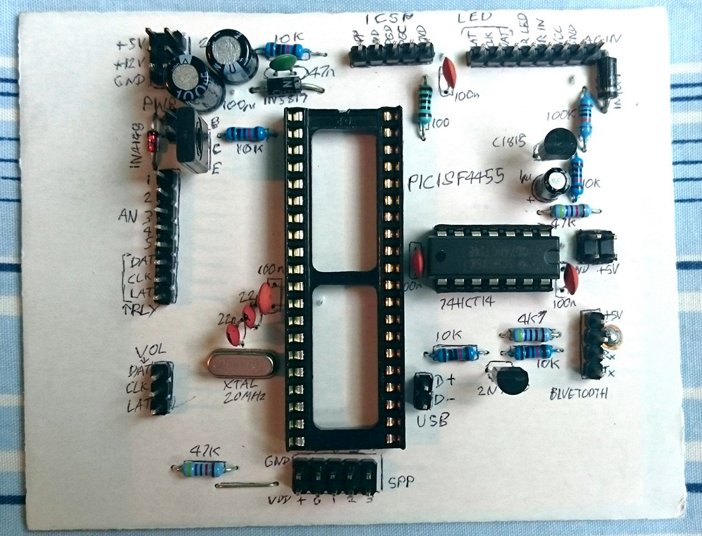
Control PIC PCB top view
To prevent the top ground plane shorting with the pins that do not connect to ground, I used a wider drill bit (2mm to 3mm) to gently drill down enough to scrape off the copper, but not too far otherwise I'd end up with a larger hole.
Vias were installed where needed to connect the top layer to the bottom - there were about 4 of those and the offcuts from the leads of capacitors or resistors I used to solder in both ends. Once the vias were soldered through the ground plane, I then covered the top of the board (plane) with another clean industrial sticker.
Built into the board too is an ICSP (in-circuit serial programming) header. Using the solution suggested Kanda (reference below), the header allows me to quickly plug in my UsbPicProg and burn the code on there, without fiddling to remove the physical IC itself and move it to another board (like I used to). The ICSP header exclusively gives power to the PIC only, and the rest of the 5V circuitry is isolated by the diode. This is to protect the programmer from overloading.
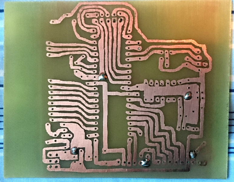
Control PIC PCB bottom layout
IR sensor/receiver, IR LED, Bluetooth and Tri-colour RGB LED
I etched another board to fit these components. The layout was constrained to have the RGB LED, IR sensor and IR LED in positions that were already drilled from the previous versions, but rather than reuse the three (quite crude) boards I had before, I created one to hold all three I/O hardware for neatness.
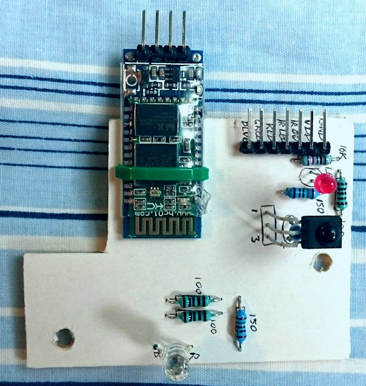
IR, RGB LED and Bluetooth PCB
This board has 2.54mm connectors for a 7 pin DuPont connector - giving me +5V, 0V, and signal lines for IR output, IR LED in, and RGB LED signals. The correct resistors to drop the 5V signal voltage for the LEDs is installed on the board, and the TSOP4838 IR sensor also has some power supply smoothing as per the datasheet and pull up resistor.
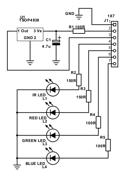
IR and RGB LED Schematic
The board also has a space to mount the Bluetooth module JY-MCU HC-06, which has no mounting holes of its own. Two small holes in my PCB and a tightly clipped cable tie keeps this in place fine, and the JY-MCU HC-06 already comes with a 3.3V regulator and PCB header installed for easy connection. The hardware to pull the 3.3V logic signal sent by the Bluetooth module is on the PIC board itself (schematic below), and the Bluetooth module seems to be fine receiving a 5V logic signal from the PIC itself without additional hardware.
To interface with the Bluetooth module, which takes 3.3V logic (not 5V), I had to implement a level shifter. The Bluetooth module is quite happy to receive 5V logic from the PIC, but the PIC will not read 3.3V logic into its RS232 receive port.
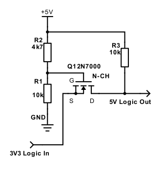
Logic level shifter - 3.3V to 5V
The level shifter I used (reference below) shifts that 3.3V input up to the VCC used on the PIC (so 5V, or 4.6V in my case). However, since the 3.3V regulator is all on the PCB of the Bluetooth module, my level shifter could not easily obtain it, so to drive the Gate of the MOSFET I used a voltage divider with 4k7 and 10k resistors to make the 3.3V approximately. This works fine.
Update: As of July 2022, I'm no longer using the Bluetooth. 99% of the time, it's not connected so just consumes power unnecessarily (actually the Bluetooth consumes less power once paired). I might bring it back, but for now the Bluetooth module is disconnected to save a little on the electric bill. Advanced amplifier settings that used to be set via the Bluetooth Android app are now set with a new function menu that can be accessed via the standard IR remote by pressing and holding the mute button.
IR remote control
This I didn't build, but spotted a remote control built by 'One4All', named Zapper URC6210. It's discontinued now, but you could do the same with alternatives.

One 4 All Zapper
It's a universal remote, which is aimed at controlling TVs. I opted for the Philips RC5 IR protocol as it is old enough that modern TVs and equipment isn't likely to conflict, and that it is simple enough to program for and likely that all universal controls support it.
I picked the very first 'code' from the list of code in the instruction booklet under the Philips header, and it worked straight away.
The remote gives me volume up/down and a 'channel' up/down, which I use to flick between different audio inputs. It also does Power and Mute. And that's all, but that's all I need so extremely convenient!
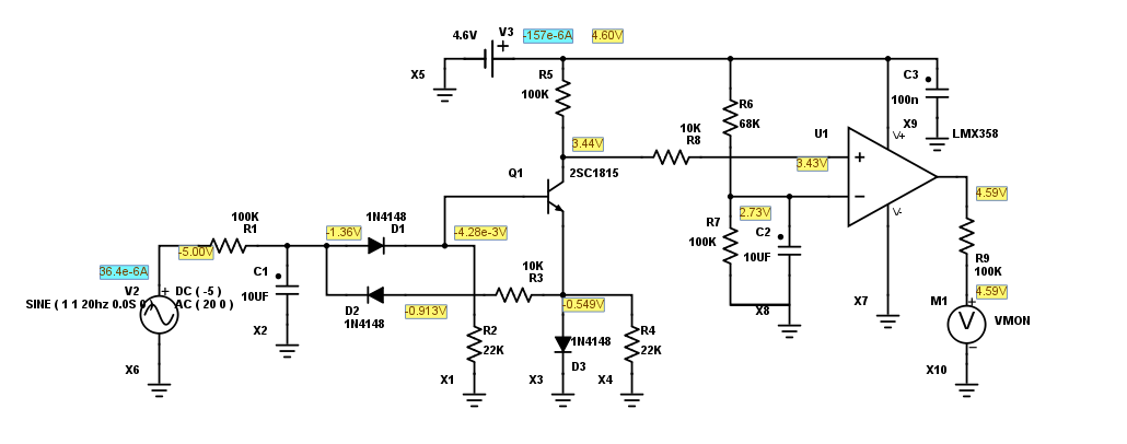
AC detector
The function of the AC detector is to detect if the mains power has been switched off. This then allows the PIC to use the remaining power still in the 5V power supply during the brief time before that collapses too, to write the contents of itfs variables to memory (EEPROM).
Doing this means that after power loss, the current volume level, input selection, surround setup etc is saved so it can be read back from memory once the power returns. EEPROM only has a finite amount of write cycles, so it makes sense to write to it only when needed.
The loss of AC detector connects directly to one of the transformer's AC outputs (low voltage, not the mains), before the bridge rectifier, and monitors that half-wave AC signal. As soon as that AC signal stops, the 1 μF capacitor will drop the voltage pretty quickly and the output from this circuit will go high.
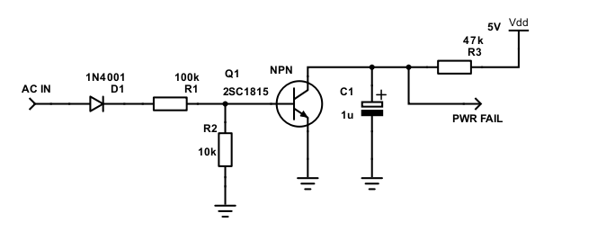
Loss of AC detector schematic
The PIC then detects this input going high (on RB0) and an interrupt routine immediately starts, and the PIC will start writing its variables to memory. This only takes a few milliseconds so completes long before the 2x 2,200 μF capacitors in the 5V PSU discharge to an unusable amount.
This circuit converts the AC into a rectified DC voltage, which switches the transistor on, pulling the output low. Upon loss of AC, the output is pulled high, but since the AC is switching on at 50Hz (or 60Hz), the 1 μF capacitor has enough of a time constant to keeps the logic level low.
Since it is not a clean 0 or 5V logic high/low, the output of this circuit must connect to a Schmitt trigger input. The RB0 to RB2 interrupt on change pins on the PIC18F4455 are Schmitt inputs, but if your microchip is not, then a 74HCT14 can be used to buffer the output. I'd initially done this, but having read the PIC's datasheet more carefully, realised it was not required and I left it out of the final solution.
The transistor is any common small signal NPN transistor. I have lots of 2SC1815 (C1815) transistors so used one of those, but a BC547 or similar will also do fine.
Speaker DC detector and mute relays
This circuit has already been mentioned on the power amplifier page, so more details are there. The comparator on that circuit will send a high signal if everything is OK (no DC detected on amplifier output), but should it go low due to a fault, the PIC will detect that (on RB2) and fire an interrupt routine which immediately switches off the relays, and then inform the user.
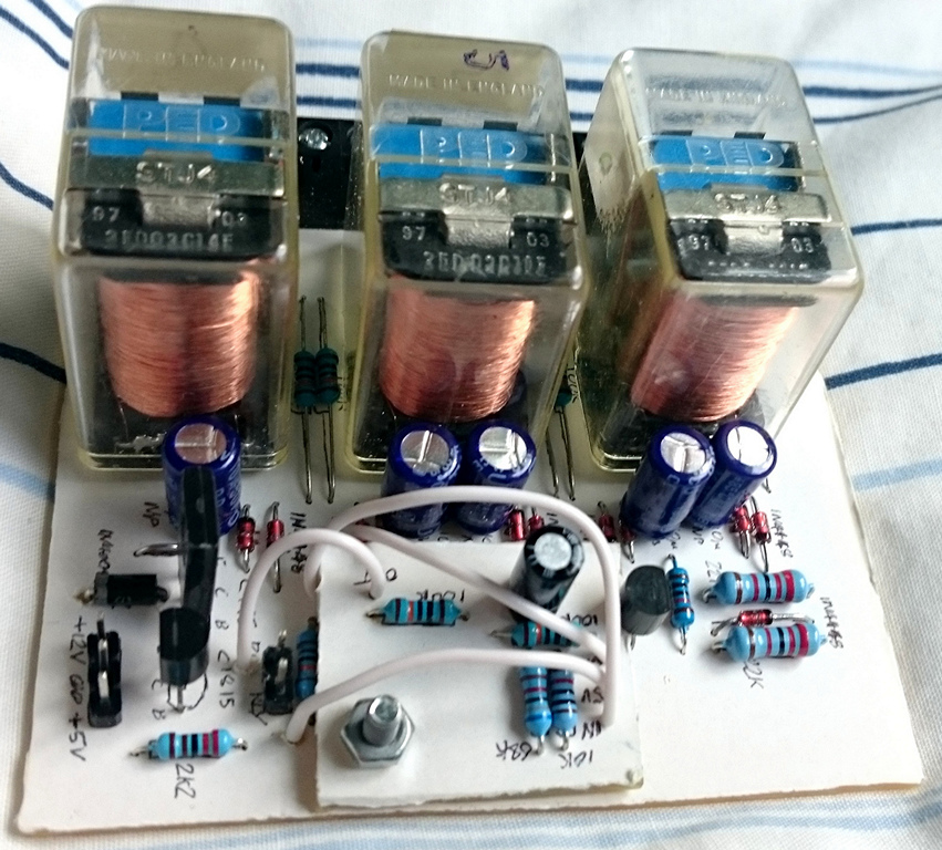
DC Detector and relay switch
The PCB that has the DC detector also has the relays, and the necessary transistors to trigger those relays from 5V logic. A two-pin DuPont connector goes between the PIC board and the DC detector/mute relay board for the DC detection signal (IN) and mute relay on (OUT).
DC detector schematic, one channel. R1, C1, D1, D2 should be replicated for each channel.
7-segment LED displays interfaced via MAX7219
These are eight-character 7-segment LED modules I purchased off a well-known auction site. They work well and are good value for money, but I question if they are genuine at the cost.
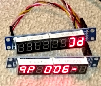
LED 7-segment modules under test
Update: July 2022 I've revised the connections to the MAX7219 modules and added a PNP switch to power them on/off.
The two are daisy chained, so I could drive both with the same 3-pin serial signal from the PIC. The modules already came with PCB headers for my DuPont connectors, and also had 'out' headers, but you shouldn't actually use them for daisy chaining (except the data pin) due to the voltage drop caused by a diode in each module, and the extra length of the clock and load lines.
I originally added stability components to help avoid nonsense being displayed on the second display, but it wasn't perfect. I now switch power (VCC) to modules on/off with the main amplifier power, resetting any corruption, and preventing it happening when the amp is off and doing nothing anyway.
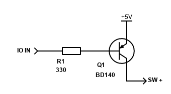
A PNP transistor switch for powering off the two MAX7219 displays.
Note: the DC current gain (hFE) of power transistors is quite low, so be aware that the base current will increase for each additional module and potentially overload the microcontroller pin, so if you have more than two modules, consider a logic level P-channel MOSFET or Darlington transistor. The BD140 is what I already had. Verify the base resistor needed, I use the transistor base resistor calculator linked below. Current at the PIC port would then be 5V divided by the base resistor, e.g., 5 / 330 = 15.2mA - which is safe (25mA is the limit for the PIC18F4455).
Why not a MOSFET? I tried with an N-Channel to switch the ground, but the MAX7219 displays do not fully turn off, so I have to switch the VCC instead. Small P-Channel logic level MOSFETs are much harder to obtain.
To daisy chain the two modules, I made a Y cable. The first 5 pin DuPont connector has two cables crimped into it for all connections except DAT. The +5V (VCC), GND, CLK and LOAD lead to the microcontroller board, and the second module. The second 5 pin connector has the DAT input coming from a separate cable leading to the DAT output from the first module, like this:
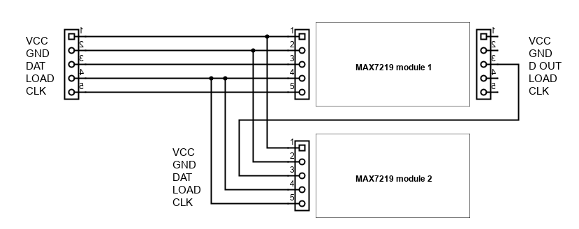
MAX7219 daisy-chain module connections
Volume control 3x PGA2310 on preamp board
The PGA2310 chips are driven by a serial signal, and the three are daisy-chained. This allowed all three PGA2310s (six audio channels) to be controlled by a 3-wire interface.
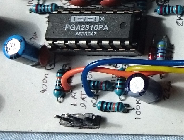
PGA2310 chip in place on preamp board
When daisy chaining, my preamp board has been setup to have the one header for the 3-wire serial circuit but has jumper wires on the board to link the other two PGA2310 chips in the daisy chain setup described in the PGA2310 datasheet.
This is done by sharing the CLOCK and LATCH lines (parallel all three lines to the chips), but the DATA line comes from a dedicated DATA OUT pin on the PGA2310 chip and goes to the DATA IN pin of the next chip.
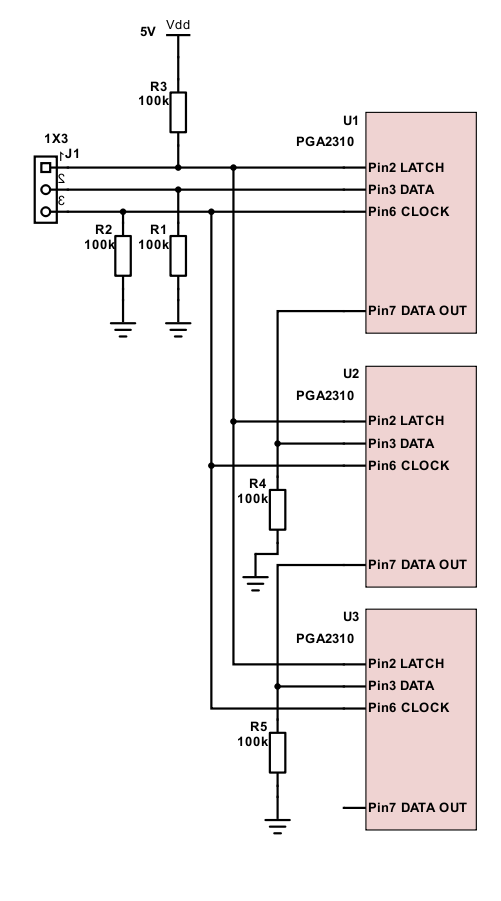
PGA2310 daisy chain
Pull up/down resistors for reliable operation are included, and I've not deviated from the original circuit by Mark Hennessy. This makes sense because DATA and CLOCK lines should be generally at logic low, and the LATCH line should be generally pulled to logic high.
Audio input selection relay control and 12V triggers
There are 5 relay signals needed on the preamp board (6 relays total, but 2 share the same signal due to switching a 4-channel signal). There are also two 12V trigger signals I wanted to include for future use.
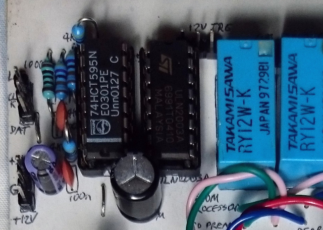
74HCT595, ULN2003A and relays in place on preamp board
Having 7 signal wires from the PIC isn't needed - a serial driving shift register can be used, such as 74HCT595 (74HT595 will also work). This takes a serial signal (8 bits) and latches it onto a parallel output. This gives an 8-pin output, driven from a 3-pin input.
To allow this parallel output of 8 pins (only 7 pins I used) to drive 12V relays and triggers, rather than use 7 transistors (and protection diodes for each), a ULN2003A Darlington transistor array has what's needed in a neat package. It has 7 inputs and outputs. One less than the shift register output, but enough for my needs.
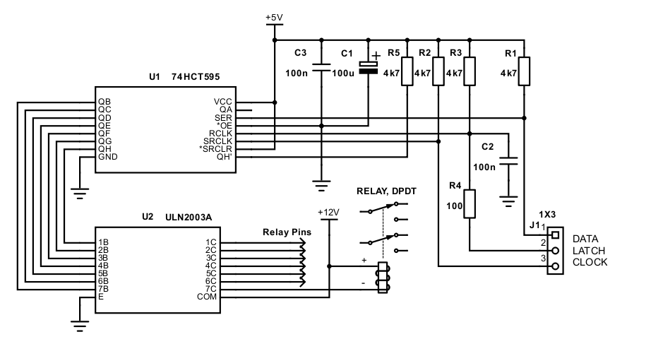
74HCT595 and ULN2003A Relay Driver
On my original build, I found that the shift register would sometimes be sensitive to noise. This would usually occur when plugging another appliance into a mains socket in the home, which would cause the relays to flick state so something random.
After research, I found H&S Tech website which described a solution that just basically adds a low pass filter (C2 and R4 on my schematic above) on the LATCH line. This solved my problems after applying it on to my old board and was incorporated into this redesigned board properly. All inputs are pulled to logic high by 4k7 resistors as per H&S design, but for CLOCK and DATA it probably won't matter, and you could pull them low instead.
Soft-start relays for power on/off
My (somewhat vintage now) soft-start circuit needs a 12V voltage to operate. I included a power transistor on the PIC board itself to drive that 12V output, so I can connect this directly to the soft-start circuit board. The PIC output switches this transistor on or off.
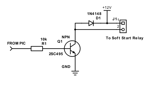
NPN Transistor Switch
The transistor switch is very generic. Any reasonable NPN transistor will do - I had 2SC495 in the parts bin but it's really old so BD139 or similar will be fine - something that can switch an amp or more. The diode is there to protect the transistor from relay reverse EMI (fly back voltages) from potentially destroying it and is required. 1N4148 will do.
TV/USB power detection
Update: This feature was added in July 2022. Having already added this feature for my STA540 amplifier, I decided I would also add it to my main amplifier.
Pretty much any TV in the last 15 to 20 years can come with a USB port, or one can easily be added with an old fashioned PCMCIA to USB card fitted into the CAM (conditional access model) slot.
A USB port can provide 5V with at least 100mA current. This would be present when the TV is switched on and will turn off when the TV is turned off. By running a USB cable to the amplifier, an opt-coupler such as the 4N25 can be used as a detector. Connecting the TV's USB to an opto-coupler in this way is ideal because it can be a completely isolated connection (therefore avoiding ground loops with the TV), and the opto-coupler's internal LED is a very light load for the TV itself, so won't damage it.
Do note though that the LED inside the opto-coupler is a diode, so you must connect the USB +5V and ground leads as appropriate. The data leads are not needed.
The other side of the opto-coupler is a transistor. The emitter can be in the amplifier's digital control ground, and the collector pulled up to the amplifier's +5V digital PSU via a resistor (4k7 to 10k will work fine). The collector also connects to the microcontroller's input pin (in my build, pin 29 RD6).
When the USB input is powered, the opto-coupler will pull it's collector output low and the microcontroller can detect this and run the power on routine. When the TV is powered off, the USB power is removed and the output of the opto-coupler is pulled high again, allowing the microcontroller to run the power off routine.
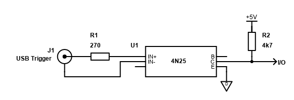
USB power opto-coupler
It's a good feature for the cost of a cheap 4N25 component, two resistors, a USB B female port (or 2.1mm DC socket) and a spare pin on the microcontroller. Chances are you already have a spare USB A to B or 2.1mm DC cable!
Conclusion
I think I made good choices with the hardware used for the control circuits. It all operates well, isn't bulky or power hungry but has allowed me to control everything from a single microchip, which can listen for inputs from an IR remote control and a Bluetooth app (although I no longer use this).
Read on to see how I put together the software to effectively communicate with all the hardware above.
References and more reading:
PIC 18F4455 Datasheet
PGA2310 Datasheet
74HCT595 Datasheet
ULN2003A Datasheet
Mark Hennessy's preamp
74HC595 Noise solution
ESP Project 111, for DC detector design
Level shifter
Forum with solution to MAX7219
stability, post #38
PIC ICSP Circuit
Peter Vis - Transistor Base Resistor Calculator
Further pages here...