
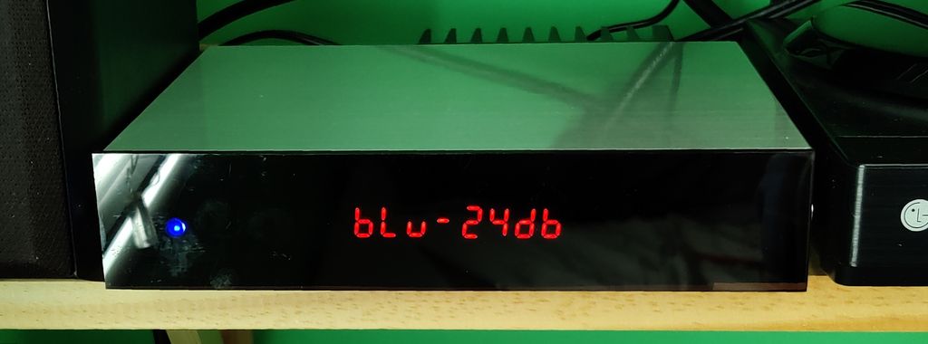
TDA7439/STA540 Amplifier - a small yet high quality amplifier
Part 1 - intro and hardware, Part 2 - software, Part 3 - conclusion
Part 1 - Introduction and hardware
My small bedroom TV previously used a PAM8610 amplifier with a passive bass boost circuit before it to drive the small Eltax speakers to a reasonable quality. It worked well, but there were three separate boxes required (the PAM8610, the bass boost and a USB power relay) in order to make it convenient. It also only operated from the TV's headphone socket, requiring the TV to control the volume, and hence it wasn't particularly noise free.
I had many of the components and software code I need though to make a small, yet pretty powerful amplifier. I also wanted to learn about and use the TDA7439, a small but convenient chip which is a preamp, volume control with balance, and three tone controls in one.
The STA540 I'd already built and wrote up an article here. I brought a universal 95W laptop PSU which gives selectable output voltages. Without any laptop PSU adaptors, it fits a standard 2 pin 2.5mm DC connector, though I brought an adaptor to convert the shorter plug to a longer reach plug for the sockets I have. This 95W PSU will power the whole system.
The design goal was to keep it small, yet still powerful and convenient to use. The features I included was:
- Remote control - I wanted the amplifier power, volume, mute and input to be controlled remotely, allowing it to be placed near the TV.
- Bluetooth - when not watching the TV, I wanted to provide a convenient way to connect Smartphones and Laptops, without having to hook in long 3.5mm audio cables (especially as these days phones are even now missing 3.5mm outputs)
- Auto-power - when the TV is powered on, I want the amplifier to power on automatically, as well as off automatically, but still have the choice to power on the amplifier individually.
- Keep the power supply requirements simple, and power draw low, especially when idle.
- Fit the whole solution in a small but smart looking case
As always, I reuse many of the parts I already had, but I did buy the case, PSU, heatsink and TDA7439 specifically for this project. This was all done during the Coronavirus pandemic in 2020/2021, so the parts I did buy were planned ahead to allow time for the parts to arrive.
The build I'd say took me more than 12 days, spread out over many months. Typically, time in a build breaks down into research and design, searching for parts / components to purchase, designing and etching PCBs, soldering and crimping cables, drilling / cutting the case and heatsink, coding and testing / fixing. This cycle repeated when I wasn't happy enough with my first design.
Design
I always start from a design, based on my own requirements. This design covers two areas:
- Circuits / Schematics - for the STA540, TDA7439, PIC16F873, power supply and accessories
- Case design - drawing a layout on paper in 1:2 or 1:1 scale so I can verify I can fit all the electronics in the cases I planned to buy
For the circuits, I originally designed and built the system mostly all on one PCB. However, the noise was unacceptable, and my redesign was to build four PCBs:
- TDA7439 preamplifier / audio processor PCB
- PIC16F873 microcontroller circuit for control of the TDA7439, display, LEDs and Relays. This board would also contain the IR receiver and IR activity indicator LED, and a 5V / USB trigger using 4N25 optocoupler
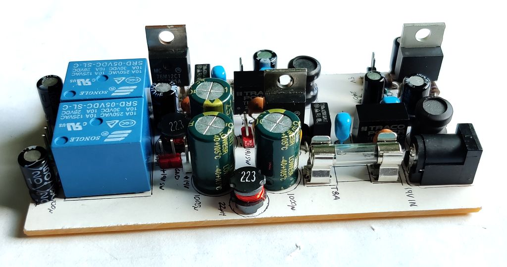
- Power supply PCB, featuring
- 2.5mm Input Socket and Fuse
- Filtering capacitors and inductors
- 2 relays - 1 controlling the power to the STA540 and TDA7439 circuits, 1 controlling power to the Bluetooth audio module
- 2x 7812 'pre' regulators
- 1x 12V to 12V Isolated DC-DC converter, followed by an LM317T set to 9V - all for the TDA7439 power
- 1x 12V to 5V Isolated DC-DC converter - for the Bluetooth module power
- 5V PSU board for the microcontroller (7812 regulator, followed by 7805 regulator)
- STA540 power amplifier board, from the STA540 article
- 1x Bluetooth audio module (prebuilt module)
- MAX7219 display (prebuilt module)
- 3x 3.5mm stereo audio input sockets and 2.5mm USB 5V trigger socket
The TDA7439 board is covered in my article here. For other boards I'll detail the design below.
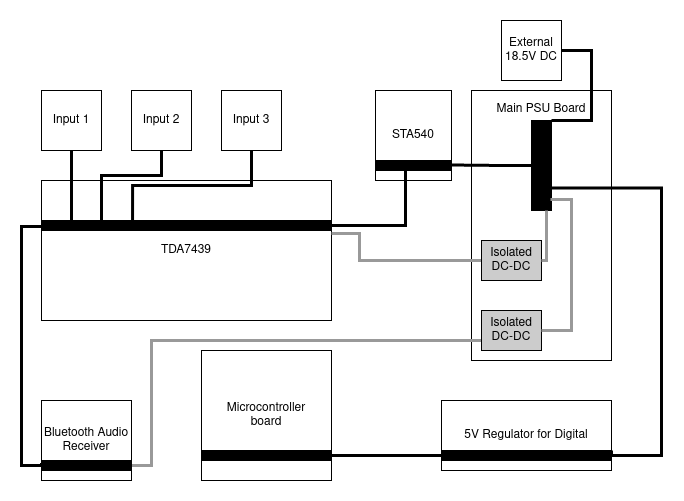
Power supplies / voltages
The entire amplifier would be powered by an 18.5V laptop PSU. These are good quality and safe to work with, however whilst 18.5V is ideal for the STA540 to deliver a decent amount of power (more than 20W per channel into 8 ohms), it's not ideal for the TDA7439 or digital electronics (PIC, display, Bluetooth).
My strategy to get 9V for the TDA7439 would be to use a LM317T linear regulator. The power consumption of the TDA7439 is very low, so a linear regulator is fine. It doesn't even need a heatsink. Plus, with my design the TDA7439 is only powered on when the amplifier is powered on so in standby there is no loss at all on this regulator.
Connecting the LM317T directly to the same PSU that drives the amplifier though creates a ground loop. This can be solved in several ways:
- Isolating the loop at the audio connection between the TDA7439 and STA540 using audio transformers
- Isolating the loop at the power supply using either a separate PSU, or an isolated DC-DC converter
- Dropping a 10-22 ohm loop breaking resistor into the TDA7439 PSU ground or audio output
- Redesigning the entire system to use a single PCB and effective ground layout
I used the second option. This gives the best noise performance and although it's some additional cost financially, it's only around £20 for the PSU and any audio quality isolation transformers (the first option) will cost more. Most 1:1 transformers will degrade the audio. Loop breaking resistors can help but are often an experiment and don't always cut noise enough. Option 4 needs a deep understanding of PCB design and grounding knowledge and somewhat out of reach to the hobbyist!
So, to clarify the requirements of the PSU...
- Filtered and fused +18.5V, switched for the STA540
- Switched isolated 9V output for the TDA7439
- Switched isolated 5V output for the Bluetooth audio module
- 5V output for the microcontroller, LEDs, IR module, relays and MAX7219 display
This is the schematic I came up with, and used in my final design:
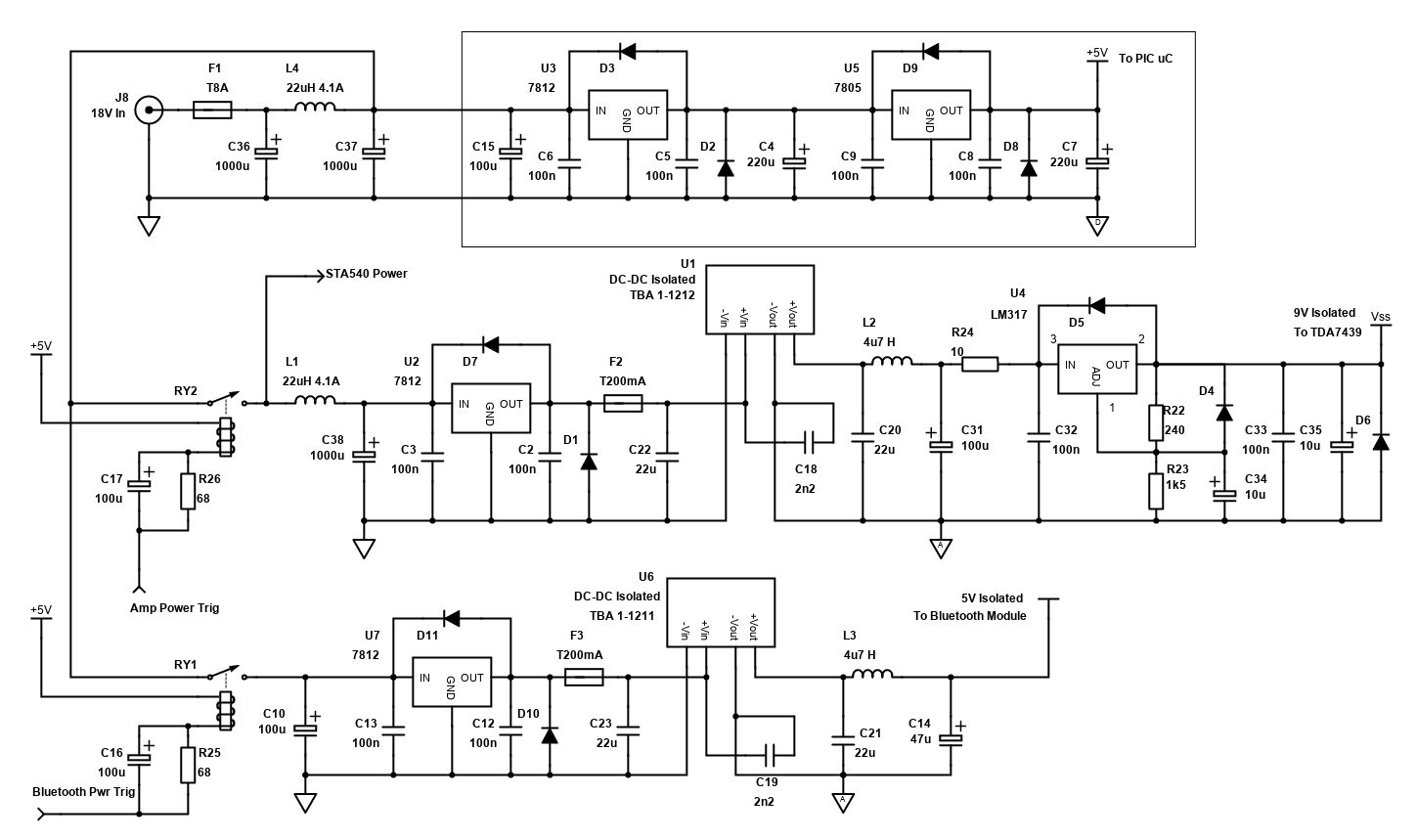
To describe this... the input from the 18.5V laptop PSU is in the top right and an 8A slow blow fuse is immediately in series with that. Although these PSUs are likely overload protected anyway, it's good to include a fuse for extra protection.
Following the fuse is a Pi filter, made up of a high current 22µH inductor and two 1000µF capacitors. This forms a low pass filter. At high frequencies, such as the switching noise from the laptop PSU, the inductor and capacitors are high impedance and therefore these high frequencies do not pass (actually considerably reduced). The cut-off is 1 / (π * √(LC)), about 2.1kHz. This should be well below any switching frequency to minimise the chance of any resonance making the noise worse.
After this Pi filter, the +18.5V is split into three sections:
- One section goes to an always on 5V regulator (top / top right area in the schematic)
- One section goes to a switched 18.5V output and 9V isolated regulated output - this is for the STA540 and TDA7439 when the amp is powered on
- One section goes to a switched isolated 5V output - this is for the Bluetooth audio module
Microcontroller 5V PSU
Updated 19th June 2022.
The digital electronics need 5V. I originally achieved this by using two linear regulators, with typical bypass capacitors and protection diodes, using the schematic below:
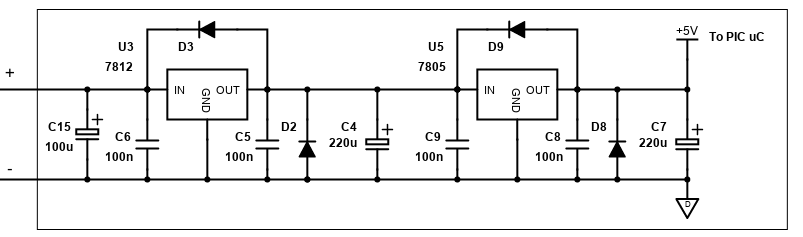
5V from 18.5V presents a problem. Using a single linear regulator would need to dump the voltage difference of 13.5V as heat. At low currents, this is possible so under standby my PIC power consumption is about 50mA - so that would represent less than 1W of heat (675mW), but when operating, the MAX7219 and relay coils increase the power consumption.
At 300mA, the regulator would generate 4W of heat, and that's a lot to get rid of in a small case and for small TO220 regulators.
I was aware of this problem and initially used a switching regulator like an XL4015 or LM2596. They are cheap and efficient, but notoriously noisy! Therefore, my initial implementation was built, on Stripboard, using a pair of linear voltage regulators (a 7812 and 7805, devices I have a lot of!).
By first regulating to 12V, then to 5V, the first regulator would drop 6.5V, the second would drop the remaining 7V. This halves the heat generated per regulator, and they can have smaller heatsinks as a result and last longer. The overall heat generated by both is still 4W, but it's now generated in two different locations. Two regulators in series have the additional benefit of improved noise ripple too.
In reality, my operating current is much better than 300mA, typically around 100mA. This is because I use a relay power saving resistor and capacitor that reduces the relay current, and not all LED segments are active on the MAX7219 most of the time, reduces power draw further. This is just over half a watt of heat per regulator and with small heatsinks each they are comfortable to finger touch. In standby, they're barely warm.
Update:
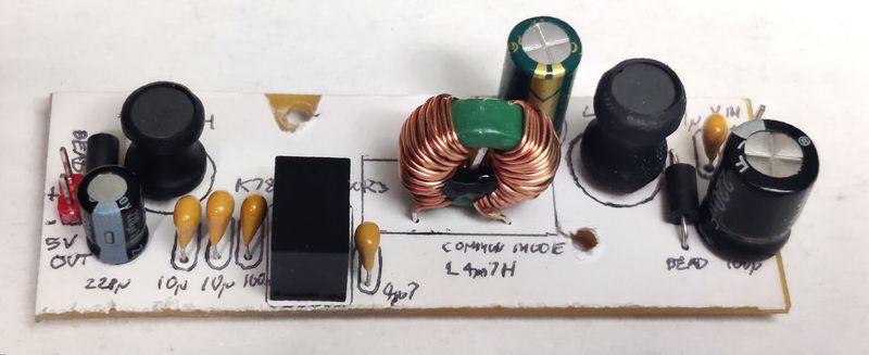
In 2022, I revised this approach though and looked at switching regulator alternatives. While I am interested in building regulators from scratch, I'm impressed with the performance of linear regulator compatible 'replacements', such as the RS PRO K7805M-1000R3 PCB Mount Switching Regulator.
This device includes a switching regulator, inductor, diode (or maybe not if it's synchronous, it doesn't say!), and other components in a tiny 3 pin package with a pin out compatible with the vanilla 7805 linear regulators. It 'could' be a drop in replacement into even existing circuits, if the space on the existing PCB is enough.
Performance is pretty good. The 520kHz average switching speed is high (10 times more than a typical LM2576), and well out of range for audio, with 25 to 75 mV peak-to-peak ripple.
Efficiency is 75% at minimum, and more like 85 to 90% generally, comparing well to linear voltage regulator efficiency of around 35% (as dropping 19V to 5V at say 100mA means throwing the difference of 14V × 100mA = 1.4W as heat, for 0.5W output). With current electric bill costs jumping hugely around the world (certainly in the UK), I'm looking a bit more at reducing standby electricity consumption around my home.
Being a switching regulator though, I was worried about noise. Not only is output noise a concern, but a greater concern is input noise. This is because the 19V input to the regulator is being used by the amp. Switching regulators generate even more noise on their input then their output and a good way of reducing noise at the input is to have filters before the regulator. Actually, there are even articles online that state that input filters are more effective at filtering the output then output filters.
I probably went a bit overboard with the filters, but the result is no noise. The amplifier isn't affected in any way, and I can still place my ear next to the speaker and here nothing (with no audio playing). A pleasing result.
The main goal of building it was efficiency. The efficiency improved so much on standby my mains eco meter couldn't even register it. Unplugging the PSU and the amplifier standby LED stays on for more than a minute.
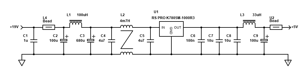
The filtering is based on some research. L1, L2, C3 to C5 are from the EMC (and EMS) compliance circuit (figure 2) from the RS Pro K78xxM-1000R3 datasheet. The common mode choke helps reduce common mode noise that the standard inductor in series with the positive voltage rail doesn't deal with. I actually used some 10mH chokes from AliExpress in my build I got some time ago. They'll do fine. I also used a higher 100µH inductor for L1 (again from AliExpress). Higher values will give better noise reduction but can resist transient current draw. As my input voltage is so much higher and my current draw is pretty constant (and low), I didn't foresee an issue.
I also added in some ferrite beads before and after the regulator. These will be effective at removing high MHz noise.
On the output, for good measure(!), I also included another inductor for filtering. This time a smaller 33µH inductor (another AliExpress order). C6, C7 and C8 are eBay MLCC capacitors from a Kit. They are cheap and probably not great performers, hence using three in parallel (a 100nF and 2 × 10µF)! This will be pretty much as effective as the 22µF capacitor suggested in the datasheet. The MLCC capacitor kit was also used for C1, C4 and C5.
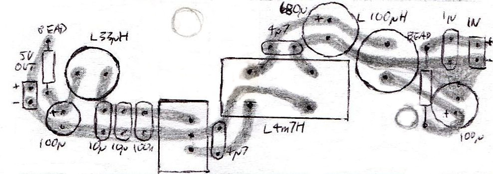
Below as a scan of the PCB layout I drew.
STA540/TDA7439 switched voltages - 18.5V and 9V isolated
This describes the middle area of the schematic. The first component reached is a relay. Relays that operate off 18V are rare. 12V is common, but I originally didn't plan on having a 12V regulator available, so I chose relays with coils for use with 5V. The Songle SRD-05VDC-SL-C can switch 10A at 30V from a 5V coil and that's fine for switching on/off the STA540.
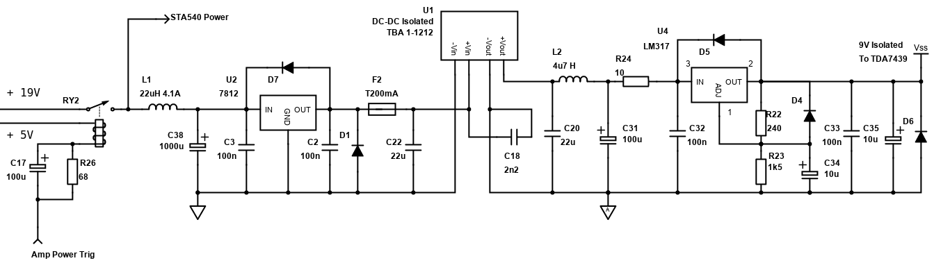
C17 and R26 are a relay 'power saving' circuit. The idea behind this is when the relay is off, C17 is not charged and will let the full current pass. Once C17 charges, it blocks DC and the DC must pass through the 68 ohm resistor instead, which limits the current.
This is fine for a relay that doesn't switch often because it gets the full current it needs to magnetise the coil and 'click' into the new switch position, but to hold the switch in position the magnetism needed is far less.
The resistor required is ([Coil voltage] - [Min coil voltage]) / ([Min coil voltage] / [coil resistance]). The SRD-05VDC-SL-C datasheet tells us that the coil resistance is 55 ohms and the drop out voltage is 10% minimum (so could be higher). I went for a safe hold (min) coil voltage of a little under half. With 2.5V, this gives (5-2.5)/(2.5/55) = 55 ohms. 68 ohms is a common value, so I went with that, which would give a hold voltage of about 2.2V. That's a power saving of over 50%, but still a very comfortable hold voltage which is recommended when the STA540 could be pulling a large current through the relay switched contacts.
After the relay is another filter (LC). This is not strictly necessary, but I incorporated it in case switching noise was coming from the isolated DC-DC converter (through the 7812) and getting to the STA540. I think it can safely be left out though.
After the filter and connection to the STA540 amplifier is a linear regulator. This provides two purposes - firstly it drops the voltage to 12V that the DC-DC converter requires. It also provides noise ripple reduction in both directions - the main concern being switching noise from the input side of the TBA 1-1212 DC-DC converter.
After the 7812 regulator is a 200mA slow blow fuse per recommendation in the TBA 1 series datasheet, and a 22µF MLCC capacitor for bypassing and noise filtering.
The TBA 1-1212 is where the isolation happens. This lovely little module is a switching converter that's uses magnetism to completely isolated the two sides. This cuts any possibility of ground loops through the power supply. The 1-1212 takes 12V input and gives 12V output. A 2.2nF capacitor was added across the +Vin to -Vout, providing a lower impedance return path for noise (following advice published by Recom Power).
As it's a switching DC-DC converter though, noise can still be generated. Although the 50kHz (min) switching frequency is outside the audio spectrum, it's still recommended to filter it so another 22µF MLCC capacitor follows the output, then a 4.7µH inductor, then a 100µF capacitor (this forms a low pass of 7.3 kHz - comfortably away from any resonance at 50kHz or higher). The 10 ohm resistor following this provides even more noise ripple filtering.
12V is still too high for the TDA7439, so the LM317T regulator and its associated components are configured to around 9V. This linear regulator has a secondary benefit of providing even more noise filtering, so the TDA7439 is getting a clean and stable 9V.
I can get away with two linear regulators and a small 80mA isolated DC-DC converted because the TDA7439 is the only device using the 9V output and it pulls at most 10mA. That's less than 0.1W heat wasted per linear regulator, and they don't even need heatsinks because of that!
Bluetooth audio module 5V isolated switched voltage
At the bottom of the schematic is the final power supply output. Again, this is switched and is only active when both the amplifier is powered on, and the input is selected to 'Bluetooth'. Therefore, Bluetooth audio is switched off when I'm watching TV or using another input directly, saving power and ensuring my Bluetooth audio isn't often available for other people's phones to connect!
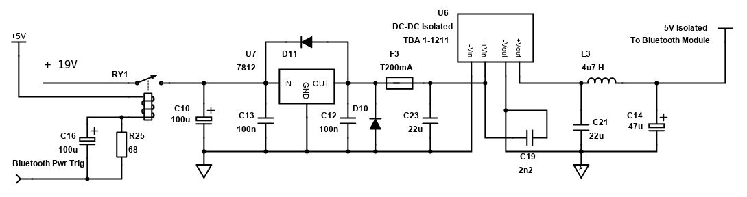
Originally, I powered the Bluetooth audio from the same 5V supply as the microcontroller, but this cause the problem of noise (due to ground) loops and excessive heat coming off the linear regulator. The Bluetooth audio module consumes less than 100mA current when on and connected to a phone.
The TBA 1 series isolated DC-DC converter helps solve any ground loop noise issues. This time instead of 12V to 12V I opted for 12V to 5V (model TBA 1-1211) to improve efficiency. I still had to use a 7812 linear regulator to drop the 18.5V to 12V for the input to the TBA 1-1211, but this should at worse generate only 0.65W of heat and a small heatsink on the 7812 is fine to dissipate most of that.
The 7812 linear regulator arrangement is the same as above, and so is the isolated DC-DC converter. The difference is no linear regulator follows the DC-DC converter, only some further noise filtering in the form of two capacitors and a 4.7µH inductor. Some additional regulation and filtering happen locally at the Bluetooth module itself.
All these PSUs need a good ground layout, so using prototype board like stripboard is not advised, not to mention a few components used will not mount in standard hole sizes and spacing anyway.
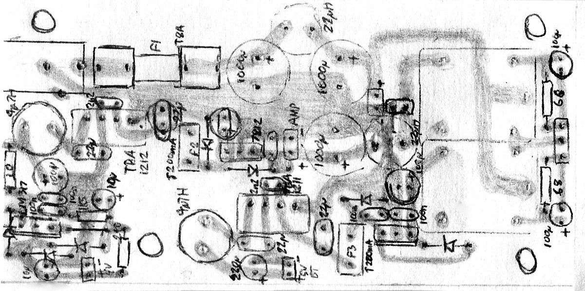
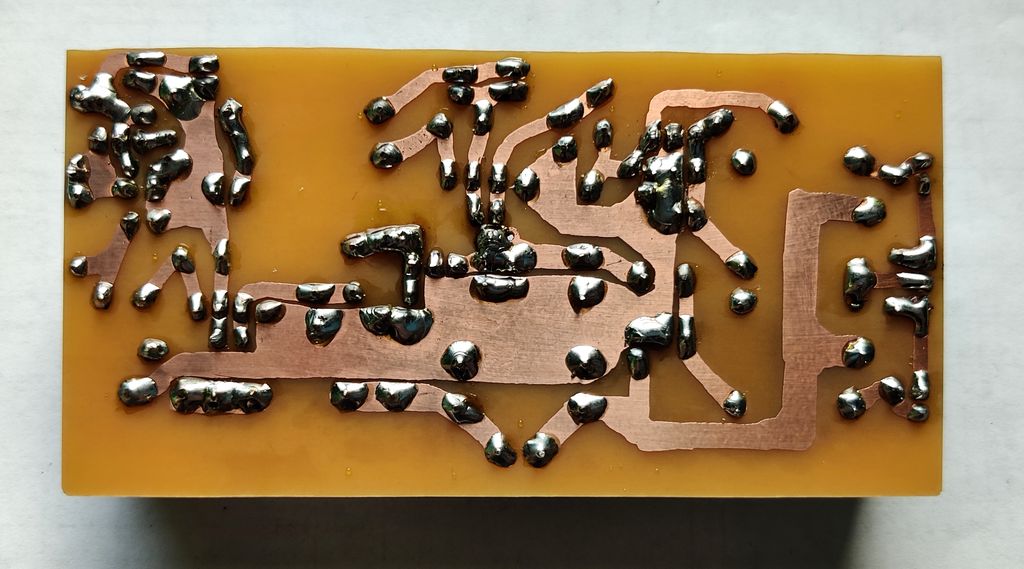
I designed my own PCB for the PSU board, taking some risk to integrate most of it on own board but the result was excellent. I made a small mistake with the layout for the LM317T, but it was easily corrected (the layout below shows the corrected version). Below are pictures of the board and layout (hand-drawn style! :-)
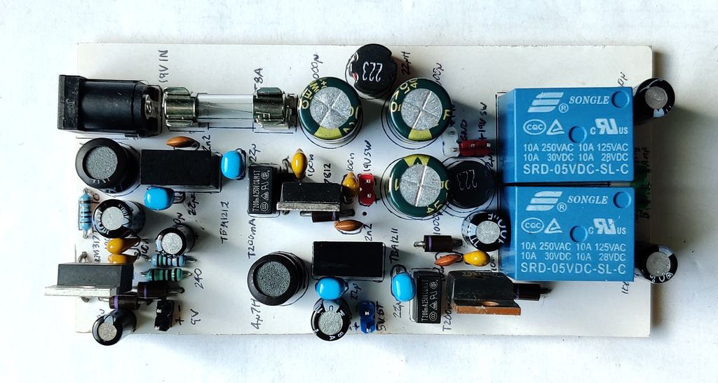
PSU PCB Layout, top view:
PSU solder side (without LM317 correction):
So, that covers the power supply! It's quite complex, but the result of the design is actually the quietest amplifier (for noise/hum) I've ever built, and that's all off just one external 18.5V voltage input!
TDA7439 Audio Processor
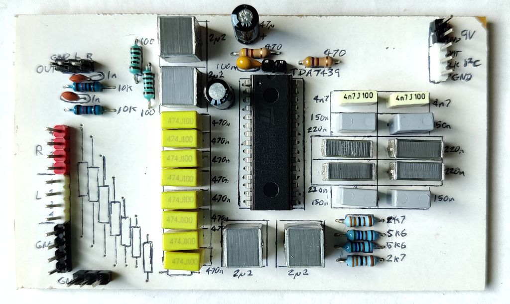
The TDA7439 was picked as a suitable all-in-one audio processor. Compared to the PGA2310 I've used before, this chip does not need separate buffers and also contains a three band tone control. It's controlled via an I2C/TWI bus rather than SPI. This means it requires less pins (two vs three), but as the address is fixed you cannot have multiple chips on the same bus and control them independently, so it's not suitable for a multichannel setup, unless you bit bang separate I2C buses for each chip.
I've written a separate article on the TDA7439 which describes the PCB and circuit details I used for this build.
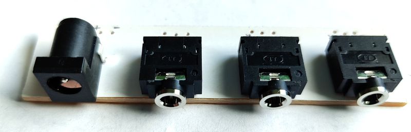
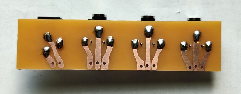
Hooked to the TDA7439 is a daughter board which has three stereo PCB mounted 3.5mm input jacks, as well as a 2.1mm DC jack for a 5V external trigger. This PCB is simple and just used for mounting the jacks.
Microcontroller
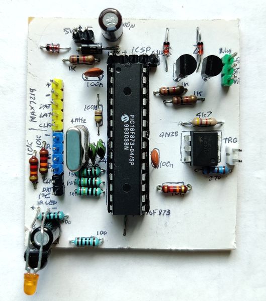
To control the TDA7439 and power to the amplifier, a microcontroller is required. The requirements for the microcontroller are not too critical.
What is does need is some I/O pins:
- 2 pins for the I2C/TWI communication to the TDA7439 (one pin must be bidirectional)
- 3 output pins for the serial 'almost but not quite SPI' communication to the MAX7219
- 1 input pin for the TSOP4838 infrared receiver
- 3 output pins to control the RGB LED
- 1 output pin for the IR LED
- 2 output pins for the power relays (amplifier and Bluetooth)
That's 12 pins in total.
In order for the infrared receiving code and the I2C code to work correctly, the speed/clock must be at least 4MHz. Finally, to save settings so that my preferences for volume, input and tone are not lost on power removal, an EEPROM would be required.
I picked the PIC16F873. Originally, I went with a PIC16F73 which I had, but I made mistakes of thinking the SSP module would help with I2C communication (it only helps with follower/slave devices, not leader) and forgetting that it has no EEPROM anyway. Having designed the PCB, I ordered a PIC16F873 as a replacement, which only just arrived as I write this, so I built the initial version on the PIC16F73 and disabled the EEPROM code.
The code for the PIC16F873 will use the MSSP module that this model comes with though, so my final solution uses hardware communication. A PIC16F1824 / PIC16F18xx would be a more modern equivalent in a different PCB design. Even a PIC16F628A would also have also worked, but with software I2C required.
The software would largely be a reuse of what I've written already for my 5.1 LM3886 amplifier and my TDA1514 / TDA2040 amplifier remake. I use the BoostC language from SourceBoost.
The PCB I designed mainly to carry the microcontroller, but it also has transistors for triggering the relays on it, the IR receiver and IR activity indicator LED, the optocoupler for powering on by external device, and various IO headers.
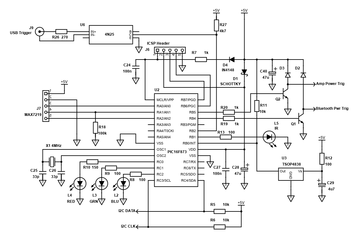
A little on each of these and the schematic...
Top left is the 4N25 optocoupler. This is designed to take a 5V input, but keep it isolated from the rest of the circuit. When 5V is present, the LED internal to the optocoupler will light (current limited by the 270 resistor) and the internal transistor will conduct, pulling the input into PICs RB2 pin low. Otherwise, when 5V is not present, RB2 is pulled high via R27, the 4.7k resistor.
Below this is an ICSP header. Normally this is left disconnected, but during development it was handy to plug the PIC programmer directly to this header and burn an updated program into the PIC.
The PIC16F873 must have MCLR pulled high during normal operation to prevent it resetting. R7 (1k) does this, but to prevent the programming voltage from powering the rest of the circuit D4 is in series with the resistor, blocking any current flow from the ICSP header to the rest to the power rail (via the resistor), but allowing the current to flow to MCLR under normal operation.
D1 is prevent the 5V power supply from the programmer from powering the rest of the circuit so that the programmer is only powering the PIC during programming. C24 is some local decoupling to improve stability when programming.
On the top right there are two NPN transistors which are used to fire the main power and Bluetooth power relays. These relays and their associated power saving capacitor/resistor are on the PSU board, but the transistor, their reverse EMF protection diodes (D2 and D3) and base current limiting resistors are on this board, connecting to the PIC I/O pins RB4 and RB5.
Off pin RB1 is an LED for IR activity. This is handy for debugging purpose, and visual feedback that the unit is receiving IR commands. It's an old fashioned orange LED from my stash, and lights normally with a 100 ohm current limiting resistor.
The IR receiver, TSOP4838, hangs off I/O pin RB0. This is configured as an input pin, with interrupt on change. All IR receivers I've seen should have a pull up resistor (R11/10k), and when they receive valid activity (i.e., 38kHz modulated, non-constant messages), pull the output low. The voltage supply is limited through a 100 ohm resistor and bypassed with a 4.7uF capacitor.
At the bottom are the I2C outputs. These are pulled up by 10k resistors (R5 and R6), and lead to the TDA7439.
Off RC0 to RC2 is the RGB LED, and current limiting resistors.
The PIC16F873 doesn't have an internal oscillator, so a crystal (or RC oscillator) needs to be connected to OSC1 and OSC2 and decoupled with 33pF capacitors.
Finally (upper left), there's a header to the MAX7219. The latch line is pulled low via a 100k resistor for stability.
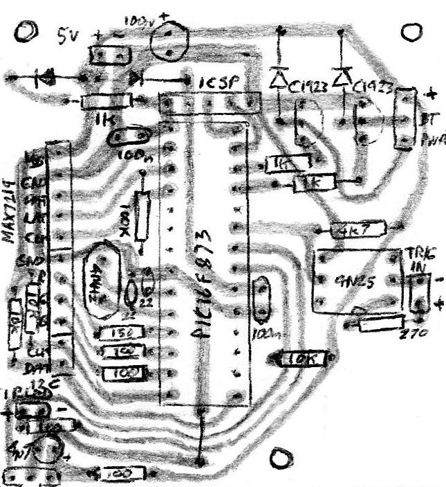
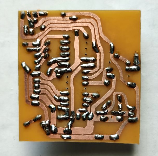
I built a custom PCB for mounting all the parts so I could be flexible with the layout and keep the size small. This is one board that could have been stripboard for simplicity, but since I would have been etching another three boards anyway...
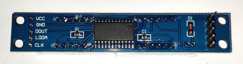
Control board PCB Layout, top view:
Control board solder side:
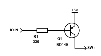
Update: I found that the MAX7219 would eventually stop working over a period of days, displaying only some characters. This is probably some noise getting on the load, clock and/or data pins, even when the amp is off.
The MAX7219 datasheet has no details of how to 'reset' the display, so I figured the best thing to do was to include a transistor switch to enable or disable power to the module when needed. A simple PNP transistor such as the BD140 will happily switch 180mA current, which is the maximum current draw of a single module. I managed to drill and mod the PCB to put the transistor in, with the base connected to the PIC pin RB3 via a 1k resistor, emitter in +5V and collector leading to a pin for connecting to the MAX7219 VCC pin.
The base resistor R1 should be calculated carefully based on the worst case DC current gain (HFE) of the transistor. I use the transistor base resistor calculator linked below. Current at the PIC port would then be 5V divided by the base resistor, e.g., 5 / 1000 = 5mA - which is safe (25mA is the limit for the PIC16F873). A 330 resistor (shown in the schematic) is better if powering two displays. For more than two, a high gain or darlington pair PNP transistor will be required.
Why not a MOSFET? I tried with an N-Channel to switch the ground, but the MAX7219 still doesn't fully turn off, so I have to switch the VCC instead. Small P-Channel logic level MOSFETs are much harder to obtain.
The PIC software pulls RB3 low when the amplifier is powered on, allowing the PNP transistor to flow power to the display. The display is then initialised during the power on routine after applying the power. This has improved display reliability, otherwise I had to unplug the power to the amp fully, let it drain, then plug it back in to reset the display in case of corrupted data.
Software version 1.2 includes the modifications to power on/off the MAX7219 module via the BD140 PNP transistor. The PCB layout above though does not include the PNP switch, but it would be easy enough to modify yourself.
Bluetooth Audio
I didn't build the Bluetooth receiver, and a purchased Bluetooth 4.0 audio module that would meet my needs. Since I have another amp with a module, I went for a different brand to ensure their names were unique.
It's a Chinese wonder, but it works fine and is even pretty good quality. I've mixed feelings about it aurally telling me when it's powered on, connected or disconnected though!
Display / indicators
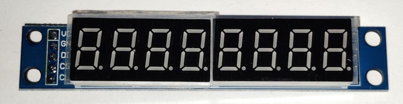
The main display is a MAX7219 module, brought online. It works, provides 8 characters, and the lit segments are red in colour. It can display eight digits on 7-segment displays. Although 7-segment displays are intended for numbers, they'll display a limited number of characters and enough for my needs.
I chose the MAX7219 display because I already have it, but also because it looks nicer than a standard LCD display and is cheaper than an OLED display. Unlike my main amplifier, I'm going to make do with only one display in this build to keep the physical size down, and avoid the wiring and software complications when daisy chaining more than one.
They'll be a 5mm RGB LED to display the status of the amplifier - red = standby, green = muted, blue = on. A 3mm LED to display IR activity will also be included near the IR receiver. Because it's a pretty bright LED, the current limiting resistor it should have (around 150 ohms) has been raised considerably to 1.8k ohms in order to stop the bright glare that happens otherwise!
A 3mm LED directly connected to the STA540 diagnostics output will also be used to indicate clipping or faults.
STA540 Power amplifier
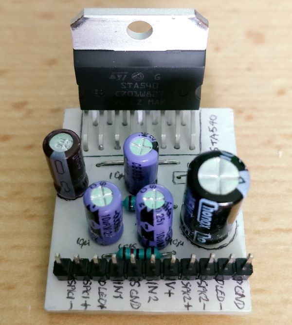
The STA540 PCB I already built would be used as the power amplifier. The article describing the amplifier and PCB is here. This delivers great sound at a pretty good volume off the 18.5V power supply I'll use.
The STA540 will be switched via a relay instead of using its standby feature (described above). Switching it via a relay ensures that the current draw when off really is nothing, and it also means I can use my existing board without modifications.
Being a Class AB amplifier, the STA540 will need a good heatsink. I brought a 1.35°C/W aluminium heatsink which is 37.5 x 160 x 40mm, however this is too long for the case, so it was cut to a length of 100mm. This will lower its performance to worse than 2.1°C/W, which is not amazing, but it's good enough for a 20W per channel stereo amplifier driving 8 ohm speakers. Under normal use, it's hardly warm.
Ground layout
Ground layout is important in amplifiers, even smaller ones like this. Because this amplifier is powered by an external switching power supply, getting the ground wrong results in a kind of horrid whine of a few kHz, instead of the more familiar 50Hz hum you'd get from a traditional linear PSU.
The power input is one ground point, which I'll call the PSU ground star/plane on my PSU PCB. From here the 18.5V to the STA540 amplifier board is directly connected to this ground point. The 5V power supply for the microcontroller is also connected here (so this is where digital and analogue grounds meet).
My isolated DC-DC converters for the 9V TDA7439 supply and the 5V Bluetooth supply mean that these PSUs can effectively be treated as separate power supplies, therefore the isolated ground from the 9V supply can go direct to the TDA7439 board, and the isolated ground from the 5V supply can go to the Bluetooth module. I've shown these, and the ground wires leading to them in grey.
These isolated grounds meet the main PSU ground via TDA7439 board, which is treated as a 'main audio ground'. The 9V isolated output goes directly to the TDA7439 board, whilst the 5V isolated output goes via the Bluetooth module board, where power supply ground and audio output ground are internally connected.
The audio signal ground from the Bluetooth module is twisted with the L/R audio outputs to this TDA7439 ground and meets where the other three inputs are connected. The TDA7439 audio L/R output is then twisted with the ground from the TDA7439 board to the STA540 board - so that's the route where the grounds meet.
This means that there are no loops, and nor is the ground wires carrying both power current return and audio return, keeping interference and distortion low.
The ground is also connected to the case via the STA540 heatsink tab (I didn't isolate it with Kapton tape or washers). The 3.5mm input jacks are isolated from the case by drilling large holes for them.
A catch though is that many laptop PSUs have their negative output earthed to the mains safety earth if they take three pin kettle or cloverleaf style mains input. This, if combined with say a TV or other Hi-Fi equipment can create a big loop via the mains safety earth if that unit is also earthed. I had this problem with my old TV but solved it by using a universal laptop PSU that isn't earthed. This has a figure-of-8 two pin mains input.
Because the DC 0V is carrying a return current, we can't use the 'loop-breaking' technique of adding a 10 ohm resistor (with bridge rectifier and capacitor in series) because under normal use there could be considerable current flowing, causing the resistor to heat and waste power.
Other options to break the loop are on the audio interconnects. Putting a 10 ohm resistor here may help, but it forces the audio return to go via the DC return and mains earth - can't be good for quality. Audio transformers would work too, or include a digital optical connection instead for TVs, CD players etc.
The ground layout and PSU design really works! As previously mentioned, it's the quietest amplifier I've ever built and you can whack up the volume right up and put your ear against the speaker and there's no hum, whine, or hiss at all. Glorious result!
References and more reading:
STA540 Build Guide
TDA7439 Build Guide
Recom Power - Very low noise filter for isolated DC/DC converters
Mousa - Power saving relay driver
ElectronicBase - Low Pass Filter Calculator
Electronics Notes - Constant-K LC Low Pass Filter Circuit Design & Calculations
Peter Vis - Transistor Base Resistor Calculator