
My 5-channel power amplifier with bi-amplified main stereo.
I suggest reading about the rebuild first. Information below is for reference purposes.
Contents
Page 1 - Idea and circuit choices
Page 2 - P3A Amplifiers
Page 3 - Crossover and Surround Channel Amps
Page 4 - Power Supply details
Page 5 - Testing
Page 6 - Improvements
Construction stages - Linkwitz-Riley Crossover
Before the signal reaches my 4 main P3A amplifiers, it first needs to be split into Bass/Mid and treble. The idea of this crossover is to begin the magic of bi-amplification. page 1 provides the details about bi-amplification and the diagram shows where in the circuit the crossover will go.
The crossover is actually made up of two boards. There is one main board which consists of all the circuitry required to make the main crossover circuit, whereas the second smaller board consists of four output buffers and controls to adjust the level of Bass/Mid or Treble. The main board also contains the voltage regulators for all op-amps onboard.
The article link is from ESP and is here. Description is:
Linkwitz-Riley alignment and phase coherent !! This is an extraordinarily nice crossover, and is
suited to top of the line hi-fi or professional installations.
However since I am choosing a configuration that is ideal for two way speakers I need components that are going to give me a crossover frequency of around 2.8kHz. This is an ideal crossover frequency for the speakers I intend to use my system with. Therefore Bass/Mid will be anything up to 2.8kHz and Treble will be frequencies higher then that.
I used the ESP component calculator for this crossover. It seems with a preferred capacitance of
33nF and a crossover point of 2840Hz (or 2.84kHz) I get the following results:
Frequency = 2840. Hz
R = 1.2 k Ohms
2R = 2.4 k Ohms
C = 33. nF
2C = 66. nF
Naturally these are the components I chose, 20 33nF capacitors in total as well 20 1.2k resistors (for good measure) and 4 2.4k resistors. All resistors are 1% metal film, however with capacitors it is extremely difficult to get any less than 10% tolerance and as I do not have access to a capacitance meter (and readings on these have limited tolerance anyway IMO), my configuration and performance of this crossover may well be less than ideal.
There were a few problems as I begun to test the board. I had found out I was missing an entire component (which was easily added after some drilling and soldering) and I had also made the board with one of the five op-amps with no connection to -Ve, only a bypass cap.. again sorted easily just by a dab of solder.
It goes to say that the layout was so complex even I couldn't avoid having some errors. It now sounds quite ok during testing.. but the crossover point seems a little lower than I expected and it also seems like one channel is behaving like a difference amplifier because any information common to both channels seems to be low. I will look at this as the project progresses.
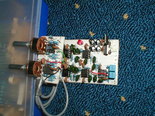
My Linkwitz Riley Crossover board, before the slight modifications to make it work
When I think of the layout at this moment, the main board in theory will be mounted on the bottom and the volume controls for low/high will be mounted above, supported by the pots. Other than standard volume controls.. this is all the input circuitry that the power amp will contain.. the rest will be in my pre-amp. In some ways I wish I had kept it all on one board as it would have made wiring a bit easier, but at least this is nearly working anyway.
LM3886 Rear Amplifiers
Designing and constructing my own LM3886 PCB was quite easy. It is a very easy amplifier to work with, provided you follow the instructions on Rod's article.
Remembering to add the extra link between pin 1 and pin 5 and having a better heatsink is the only differences you need to take into account when using an LM3886 over an LM3876. If you can pick up these chips cheap then they are well worth the effort and the cost as the rest of the circuit is cheap.
The power for these LM3886 chips comes from the same power supply as the P3A amps, except I have dedicated another bridge rectifier and a further two 33,000uF capacitors to the rear (and centre) amplifiers. This will be the same +/- 35V which is ideal.
Heatsinking comes from a large but quite thin heatsink which is cooled by fans when temperatures get quite high. Testing has so far proved that this is very adequate.
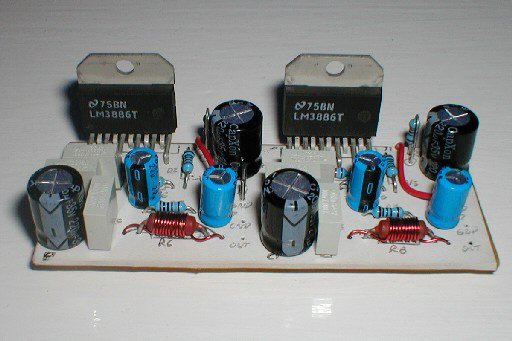
My LM3886 PCB - contains two amplifiers for each rear channel.
In heatsinking this device I took the same measures as I did when mounting the transistors for my Project 3A amps. Go back to see.
I could get away with the same mica washers used for those large power transistors, they had the correct width but I used a pair of scissors to carefully chop the excess height off the bottom.
One important thing the LM3886's need though which the onsemi transistors on the P3A did not need was bushes. This is because the screw used to mount the devices on the heatsink would short them again - making the mica washer useless.
A bush is a simple cheap solution which just allows the screw to pass through the centre of it and has a lip on one side for the screw to bolt down onto. It is very effective and solves the shorting problem. The picture below shows my LM3886 PCB mounted on its heatsink, and working.
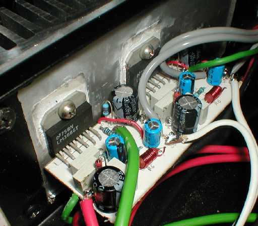
LM3886 amps correctly mounted.
TDA7293
 I have not got much to write about my TDA7293 amplifier. I chose it because I could get the
TDA7293 chips pretty cheap and I wanted to have a centre channel that could keep up with the
P3A's when needed.
I have not got much to write about my TDA7293 amplifier. I chose it because I could get the
TDA7293 chips pretty cheap and I wanted to have a centre channel that could keep up with the
P3A's when needed.
Sadly upon testing my TDA7293 circuit at first it just did not make any sound so I assumed that the mute and/or standby features were enabled. This caused me to set about disabling them, but in that process I managed to destroy my test speaker well and truly in the next test.
My poor test speaker didn't even make a sound - just smoke bellowed from the voice coil and that was its poor life over. And a very yucky smell too.
At present I have given up on the TDA7293. I will either give it another try or just migrate to another LM3886 as these have impressed me so far.