
My 5-channel power amplifier with bi-amplified main stereo.
I suggest reading about the rebuild first. Information below is for reference purposes.
Contents
Page 1 - Idea and circuit choices
Page 2 - P3A Amplifiers
Page 3 - Crossover and Surround Channel Amps
Page 4 - Power Supply details
Page 5 - Testing
Page 6 - Improvements
Construction stages - P3A amplifier
The PCB's
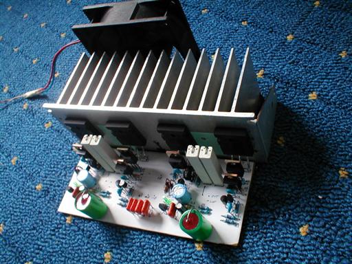
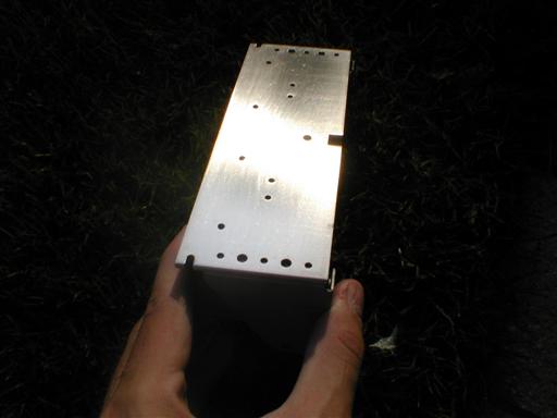
First picture I done after I completed one amp with the components I had. This shows where I will
have the fan, but at this point the P3A was not mounted on the heatsinks.
There isn't a great deal to say here. I brought one of Rod's PCB's which satisfy my need to know a good layout for the bulk of P3A circuit... I did not want any random noise or oscillation to occur and there is recent evidence of someone getting this from their own design.. which is suffer and agony for them just by not buying Rod's PCB. It is a fair bit of money.. but worth it IMO.
But anyway, onto my thoughts of the construction. I only brought one board and this will be used for neither of my amps in my complete system. I designed my own board so it would fit my components far easier and also fit my heatsink. In order to do this my fuses had to be on a separate board away from the main boards. This does unfortunately mean running 4 power wires to each stereo board rather then the two required on the original design.
Other modifications I made were the layout around the power transistors and the emitter resistors. As you can tell from the pictures below, the resistors I had, and got were 7 watt versions which have no easy chance mounting on the original PCB. I also modified the layout to get around my huge audio quality Suflex input capacitors, and removed the resistors for bridging and connecting a SIM (sound impairment monitor).
Complete Pictures:
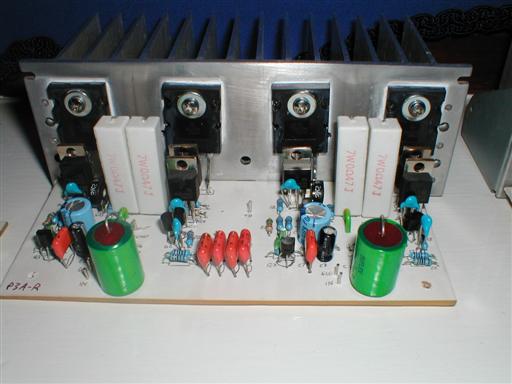
Right amp
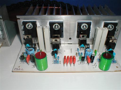
Left amp, slightly off the centre of the image :/
Close up of right amp
You may notice the 7W resistors are different on each board. Well, the longer thiner ones are the ones I obtained first, from Direct Electronics.. however I emptied the poor guys stock when I asked for 12 of them, he could only supply 4. The other ones are from maplin and I spent half an hour soldering them in a board that was designed for the other type. The maplin ones won't vertically mount without extending one of the wires, so what I had to do was chop some off one end and solder it to the other, using mere blu-tack as support. Very fiddly.. especially as those type of leads need to get quite hot before the solder properly flows onto them and stick well. I done it in the end though.
Still, assuming they work, I am happy with my PCB's so far, they look nice and will match the rest of the amp.
Heatsinks
I will go into a little detail about my heatsinks and how I performed my transistor mounting. Below are some pictures of my second hand heatsinks (apparently originally pulled from a Yamaha 50WPC amp). These are hopefully adequate enough to keep the transistors happy under normal operating conditions and with an 80mm fan on each heatsink too, demanding situations should also cause no problem... not that I would ever want to push this amp into distortion.. I fear it would blown my loudspeakers or itself :E
I forgot to do a decent picture of the heatsink before working on it.. so the first photo on this page is the best you will get.
There are some photos of my handiwork however...
This is a picture of the smooth heatsink now acting as a brilliant mirror to sunlight. This is
1/650sec exposure time! The dark background is lush green grass under one of the best
English summer days.
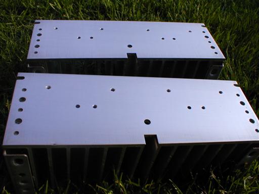
Picture of both heatsinks after sanding with P800 and P1000 sand paper. The photo makes
them look perfect, when they were actually not, but they were close and you could not feel any
different with your finger. This is still a fast exposure at 1/320sec.. it was a bright day.. rare in
England!
Mounting those transistors was a nightmare. Maybe it was the way I did it..but at least I think I have done ok. I used CPU thermal compound from the days I needed it for my Athlon K6 300, so its not exactly brilliant, but good enough as I have used it for athlon XP's and Thunderbirds. Before the K6, CPU thermal compound wasn't really needed ;)
Anyway, the first thing was to gather all the bits I needed.. those boards, the heatsinks, the mica washers and the compound. I also got a old phonecard to spread the compound as thin and evenly as possible. I had made the holes and threaded them with self tapping metal screws the day before.
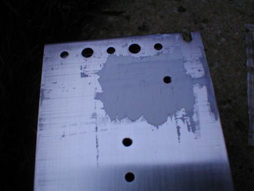
The compound really was a nightmare, it just wouldn't spread to my needs easily and sometimes
I would get close to what I wanted and then mess it up again, grr, patience essential! This isn't
really a good example and I think I improved that result before adding the washers. The idea is
simply to spread it as thinly as possible with no gaps.
Once happy, I could then place the mica washer. It has to be done in a fashion that will trap the least air as possible. Either way, sometimes that happens and if it is that bad, remove the washer very carefully (they are fragile) and then wipe off and re-apply compound. Sometimes you can get away with the odd small bubble by pressing down on the washer. They do need to be pressed down quite firmly in order to get the least thermal resistance possible.
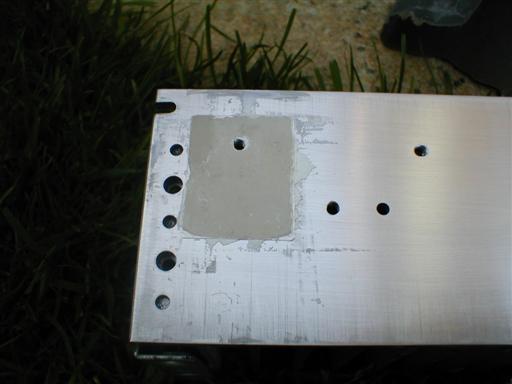
One mica washer successfully added. It looks like some bubbles are there, but these are
actually present in the washer since I brought them.
After all washers are added, it is time for another layer of compound - this is the one that sits between the washer and the transistor package. Again it must be as thin as possible.
All in all I used 1ml of compound for all 8 transistors, sounds a lot, but there were some errors and I always put more on and pushed it to the side rather then too little. I doubt I would have got my spreading any thiner without reaching the surface.
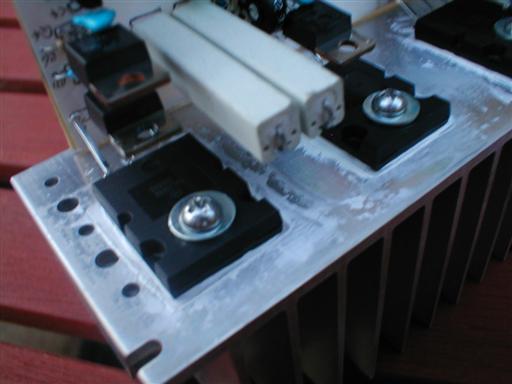
This final picture shows the result of my mounting before cleaning up the excess. I used a washer
with my screw so the pressure would be spread a little more.. too much in one point may lift the
transistor up at the bottom end and increase thermal resistance unacceptably. This is also why
Rod suggests no overtightening.
The compound is very sticky so I had to use methylated spirit to remove it, even with this I didn't do a fantastic job. However the end result is good enough looking anyway!
Fuses
I couldn't fit the fuses on the PCB, so I had to have them elsewhere. Do not even think about omitting fuses altogether! There are a lot I know, but safety is important in any project.. I do not want to hear any case of their amp causing injury to themselves or others because they had no fuses, and I bet the designer of this amp wishes never to hear this either.
So my solution was to have the fuses on a separate board... all eight of them!
Although quite big.. this is a damn simple PCB to make I didn't even need much of a template, except for hole marking.
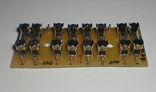
My fuse board, a simple safety measure that could not be fit on the main board. It also acts as a
handy cable splitter as I would only need two input wires, but eight output wires (two for each amp).
The input wires come straight from the PSU.
That just about does it for the P3A information.. there is a fair bit, but to get the information you really need, look at the designers site. More essential information that I cannot repeat here is also on the secure section of the site which you can only get to after purchasing PCB's (recommended). Rod's article is here.