
TDA2822M / D2822A / KA2209 DIY Guide - Simple low power stereo amplifier
Contents
Warning: The TDA2822M has now been discontinued (in its DIP package) and is susceptible to fakes. If you're buying, make sure it is from a good supplier to get the genuine chip otherwise performance may be worse.
Alternatives are
- PAM8403 for a stereo 5V USB or 4.5V battery operated use - this is a Class D amplifier, but is surface mount and you would buy a pre-built module rather than solder yourself
- TDA7266 supports 3V to 18V voltage output, is stereo, bridged, and gives much more power. TDA7297 (stereo) is another alternative, but 6V upwards only
- LM386 for a basic mono amplifier - however power output is worse
- TDA2822D / TDA2822D013TR uses the same circuit as below, but it is an SO8 package (surface mount). You can get SO8/SOP8/SOIC to DIP adaptors to aid PCB design and soldering though
The TDA2822M, and compatible alternatives such as the D2822A, KA2209B, NTE7155, NJM2073 were incredibly popular chips and often appear in low-cost battery powered consumer equipment such as radios. I've seen it more often than the LM386, and really, it's a better alternative to the LM386.
So, you may have heard of the TDA2822 or TDA2822M before, but for those who haven't, it is a small 8-pin chip that has two modest power amplifiers on it that means it can easily be either a stereo amplifier, or easily bridged to produce a more powerful mono amplifier.
Note that this article is about the 8-pin DIL TDA2822M. The TDA2822M may be named TDA2822 by UTC, but there is also an older TDA2822 16-pin variant by ST with greater power output (but a larger size) that does exist but it's a little rarer.
Recommended Experience : Beginner
TDA2822M application
Quick facts TDA2822M
- Power output stereo: 1W into 8 ohms at 10% 1kHz distortion with power supply 9V
- Power output stereo: 0.38W into 8 ohms at 10% 1kHz distortion with power supply 6V
- Power output stereo: 0.15W into 8 ohms at 0.2% 1kHz distortion with power supply 6V
- Power output stereo: 0.65W into 4 ohms at 10% 1kHz distortion with power supply 6V
- Power output bridged: 1.35W into 8 ohms at 10% 1kHz distortion with power supply 6V
- Power output bridged: 1W into 4 ohms at 10% 1kHz distortion with power supply 4.5V
- Gain: 39dB with standard application, can be adjusted down to 20dB with additional feedback resistors
- Power supply: 1.8V to 12V single supply
- Datasheet available here
Guide
I originally brought the TDA2822M as an amplifier available from Maplin at the turn of the century. It is an easily built and quite well performing amplifier for its size. I've seen it used frequently, including in radios, 'Ghetto Blasters' and in PC speakers. A pair of PC speakers I got free when I brought a computer case claimed 120W PMPO!
Well, I won't lie like they do; this amp is only capable of 380mW (that's milliwatts) per channel from a 6V power supply into 8 ohms, and that's at 10% distortion. With a 12V power supply, it'll get over 2W per channel, but it's being pushed to its limits at this voltage supply. The datasheet does not show a power output into 8 ohms above 9V - which will net you 1W per channel. This amp can also function well as a headphones amplifier, providing 20mW into 32 ohms from 3V.
So, what have I done with these amps then? My first use was to upgrade a small pair of passive Walkman type speakers. This would have been in the year 1999 when I was aged 16 or 17. I drove the TDA2822M only from 3V (2x AA was as many batteries that would fit in the speaker), but there was tons more volume then having them just passive, I recall other teenagers being quite impressed (although as you can guess the tone from the small speakers was poor).
During university (~2003) I built a slightly larger pair of speakers, but still pretty compact. A friend was impressed enough to want me to build another pair for himself too, you can read more about them here.
In 2009 I travelled a lot, so I used two TDA2822M chips to make a stereo + bridged set of speakers with a 2.5" speakers and tweeters. They passed music and TV duties whilst in hotels and apartments when I was working in Geneva, Switzerland and Tokyo, Japan. I later upgraded these speakers with a Bass Boost circuit and used them for a while in the small bedroom for TV sound (as they are much better than the built in speakers of my 26" TV). You can read more about those here.
The TDA2822M will provide 1W into each from a 9V PSU, and when bridged it will get near 2W at 7V, and with that these speakers easily impress more than most cheap PC speakers. The bigger TDA2822 (instead of TDA2822M) allows more voltage and a higher output power, but I've never built one, and this chip is even more obsolete.
The TDA2822M has a few alternatives which are basically compatible with the same performance. These include (and there may be more) the KA2209 (or KA2209B) from Samsung, NTE7155 from NTE electronics, D2822/D2822A from Silicore, YD2822A from WuXi YouDa Electronics, NJM2073 / NJM2073D / NJM2073M from JRC New Japan Radio Co. ...
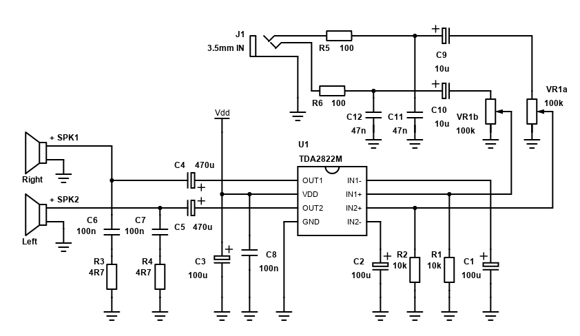
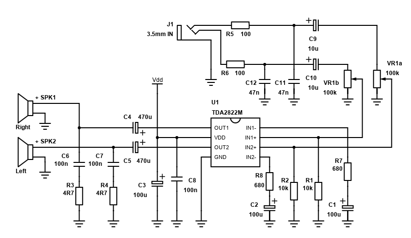
Below is a stereo configuration schematic that will work for all these chips.
| # | Type | Quantity |
|---|---|---|
| U1 | TDA2822M | 1 |
| U1 | (optional) 8 pin DIL DIP socket | 1 |
| R1,R2 | 10k ohm Resistor, ¼W Metal Film, 1% | 2 |
| R3,R4 | 4.7 ohm Resistor, ¼W Carbon, 5% | 2 |
| C1,C2,C3 | 100µF Capacitor, 16V+ Electrolytic | 3 |
| C4,C5 | 470µF Capacitor, 16V+ Electrolytic | 2 |
| C6,C7,C8 | 100nF (0.1µF) Capacitor, 50V+ Ceramic X7R or MLCC | 3 |
| VR1 | 100k ohm Dual Log Potentiometer | 1 |
| Vin L/R,+Vs,Spk L/R | 2.54mm header 7-pin (cut as needed) | 1 |
| Cable, connectors | ~ |
Optional, but recommended
| # | Type | Quantity |
|---|---|---|
| R5,R6 | 100 ohm Resistor, ¼W Metal Film, 1% | 2 |
| C9,C10 | 10µF Capacitor, 16V+ Electrolytic | 2 |
| C11,C12 | 47nF (47000pF) Capacitor, 50V+ Ceramic | 2 |
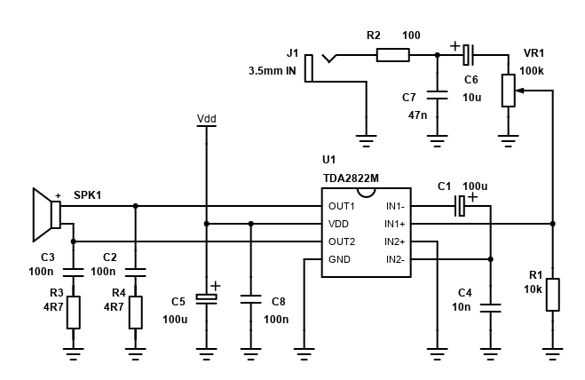
The main schematic for the amplifier consists of the bottom half of this drawing and is as per the datasheet. The volume control VR1, DC offset protection capacitors C9 and C10 and low pass filter (C11/R5 and C12/R6) are additional components I recommend for a system but are not included in the PCB layouts.
The schematic has been redrawn to match the pin layout of the TDA2822M IC (pin 1 is in the top left and it's anti-clockwise from there with pin 8 in the top right). This means that the input side of the amplifier is actually on the right-hand side of the schematic, and the output/speakers are on the left.
Power goes to pin 2 - from 3V to 12V (15V absolute max). The power supply must be bypassed with a high frequency ceramic capacitor - that's the 100nF C8 which must be as close to the IC as possible. A larger bulk electrolytic of 100µF (C3) or larger must also be present. These capacitors are polarity sensitive so ensure they are the right way round!
The TDA2822M has non-inverting and inverting inputs. There's two of each. The non-inverting inputs (indicated with the +) will go to your source - i.e., left and right stereo signal. R1/R2 are needed for a DC path to ground and to give your source a reasonable input impedance. DC offset at the non-inverting inputs is very small (I actually couldn't measure more than a millivolt) and blocking capacitors are not required and should not be used.
The inverting inputs (indicated with -) must connect to ground but because they do have a DC voltage offset, they must be via DC blocking capacitors C1/C2.
The output will also have a DC offset voltage. If our speaker is connected to the output pin and ground, this DC current would flow through its low resistance voice coil to ground, which will cause the speaker to heat up, lose performance and the amplifier to waste power. The speaker may be potentially ruined. DC blocking capacitors C4 and C5 prevent this DC flow and allow only 'AC' to pass through.
How does the DC blocking capacitor work? I'll explain one channel (pin 1 and C4). Imagine the amplifier is powered by 12V. It'll create a 'virtual ground' of 6V, and it would be able to drive a 4V peak wave (these amplifiers are not rail-to-rail) - that's 8V peak-to-peak or 2.83V RMS (for a sine wave) - calculated as 0.707 × peak voltage.
When the amplifier is powered on, pin 1 outputs 6V and the C4 charges to 6V (this causes the pop on power on). As the wave is played, pin 1 will rise to 10V, causing the capacitor to charge more through the speaker. This change in current flow through the speaker pushes the cone out.
Once the peak of the wave is reached (10V) it will reduce back to the virtual ground (6V) and then go to the inverse peak (2V). C4 was charged and now has a higher voltage than pin 1. It discharges through the speaker, causing the cone to move in the opposite direction. This constant charge / discharge of the capacitor through the speaker makes the cone move and sound is produced.
Finally, C6+R3 and C7+R4 are Zobel networks / snubbers which are needed for amplifier stability. Whilst some amplifiers do not need them, they are quite common for most amplifiers, and you'll need them to ensure the TDA2822M is stable at high/ultrasonic frequencies. Note that R3/R4 are 4.7 ohm resistors (not 4.7k ohm). C6/C7 should be 100nF ceramic capacitors.
The Zobel network is shown in example schematics in all datasheets I've seen, so I'd consider it necessary, however I do have a cheap mono radio that use a D2822A chip in BTL configuration and this omits the Zobel network, however its driving a very small and extremely awful 8 ohm 0.5W speaker! It also has a very short wire to that speaker. I guess if you were building a fixed unit where the speaker will never be changed and the wires to it are very short, you can prototype a circuit without these components and see if it is stable with an oscilloscope without very high frequency oscillations. My recommendation is to just include it and not waste time trying without - cost (price and space) of a couple of capacitors and resistors is small.
Construction
The main schematic for the amplifier (see above) consists of the bottom half of this drawing and is as per the datasheet. The volume control VR1, DC offset protection capacitors C9 and C10 and low pass filter (C11/R5 and C12/R6) are additional components I recommend for a system but are not included in the PCB layouts.
The circuit is simple to construct, and it can be done easily on stripboard/Veroboard or breadboard, but the best results for performance and size is to use a custom layout. The datasheet has example layouts (also available below) and I've added options for a stripboard layout that could be constructed by novice builders, yet still work well.
When building, make sure that you insert the TDA2822M chip in the board the right way and as well as the electrolytic capacitors the right way round. Nothing else is particularly critical, the amp will happily run with the cheapest resistor and capacitors you can buy.
Of course, ideally, resistors should be 1% metal film, but 5% carbon are also fine. Capacitors C1 to C5, and C9 to C10 are electrolytic capacitors. They must all have a voltage rating greater than your supply voltage. The maximum supply voltage is 15V, so pick 25V rated capacitors at a minimum. Use 16V capacitors only if you know the power supply will never exceed 9V. The remaining capacitors C6, C7 and C8 (100nF), and C11, C12 (47nF) should all be ceramic capacitors.
DC blocking capacitors C4 and C5 affect frequency response as they form a high pass filter with the impedance of the speaker. With 8 ohm speakers, 470µF gives a cut-off of 42Hz, 1000µF will get down to 19Hz. For 4 ohms, it's 84Hz for 470µF, and 40Hz for 1000µF. The calculation for the cutoff is 1/(2πRC) - e.g., for 8 ohms, 470µF it's: 1/(2 × 3.14159 × 8 × 0.00047) = 42.3Hz.
If the applications are for small speakers, the default value is fine. If the use case is for larger speakers and you want the low bass to come through, I suggest to go for a bridge configuration below (two amplifiers needed for stereo), since the bridge configuration does not need DC blocking capacitors and you'll definitely be needing the additional power for larger speakers anyway! Even the bridge version is still low power though and driving large speakers or subwoofers is not what this amp is really intended for :-)
Also bear in mind that bigger values for C4 and C5 are more expensive to buy and take up more room on the PCB. I would advise against going larger than 1000µF as charging these during power on or speaker connections will put stress on the amplifier.
As mentioned, I've added VR1 (a 100k dual linear potentiometer) and capacitors C9 to C10 to protect it from DC offset voltages (which will cause it to make scratching noises after some time). I've also added a low pass filter R5/C11 and R6/C12 which will help filter high frequency interference including GSM noise from mobile phones nearby. The cutoff for the low pass filter is 34kHz - that's also calculated by 1/(2πRC) - 1/(2 × 3.14159 × 100 × 0.000000047).
For VR1, a dual pot lin is recommended. This is because it is loaded by the 10k R1/R2 resistors anyway and will give a logarithmic response. You might get a better response still by using 12k resistors for R1/R2. Lin (linear) pots a usually marked with a 'B' e.g., B100k.
Including the TDA2822M chip, that's 20 components in total. If you don't need a volume control or low pass filter, exclude VR1 and C9 and C10 as well as R5, C11, R6 and C12. Anything else can be added as you require, i.e., tone controls etc., but it is unlikely you will need anything else for simple systems.
Note: Unlike many single supply amplifiers, the TDA2822M does not generate a ½ voltage DC offset at its input pin, therefore a DC blocking capacitor at its input should not be used and you can connect it directly to your source or volume control.
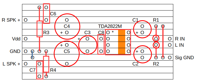
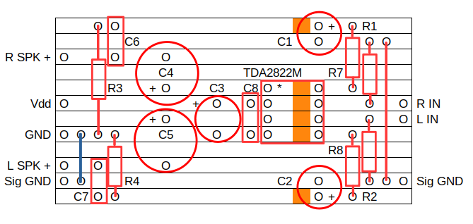
Stripboard layout
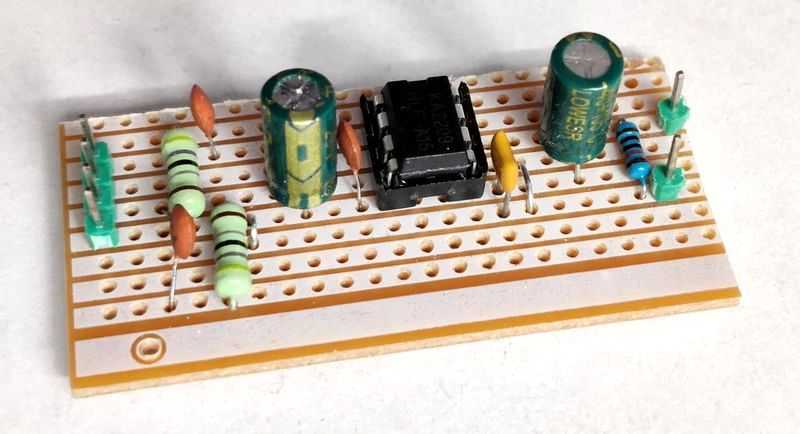
Below is my suggested layout for a stereo TDA2822M (or KA2209B as I used, or other alternatives) on SRBP stripboard/Veroboard or similar. This would allow you to build the circuit in less than an hour.
You would need to obtain a stripboard cutting tool, or use alternatives like carefully using a drill bit (in a manual or low speed battery operated drill) or knife to make cuts in the copper strips where the dark orange squares are.
Solder the TDA2822M first, or ideally solder an 8-pin DIP socket. Then work outwards from the chip so you solder the components in the correct places. Note that R1 and R2 are vertically mounted resistors. Once soldered, trim off the excess leads, but keep them.
The offcut leads can be used for the unmarked wires in red and blue on the diagram. These are known as jumpers. The jumper in blue should be installed unless your external circuit has the signal and power grounds already connected together at another point. In this case, leave the blue jumper out as installing would create a ground loop, resulting in hum or other noise.
I've not included VR1 and the capacitors/resistors before it. These are all optional and VR1 will come in different sizes and probably will be annoying to solder on to stripboard. You could create a separate board for these or wire them off a board using a point-to-point method.
Custom PCB layout
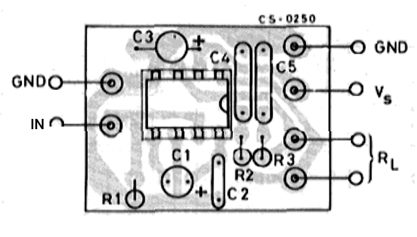
ST Microelectronics were nice enough to also provide PCB layouts in their datasheet. The following is the stereo application of the TDA2822M fit onto a very small sized board. The only problem with this is for most of my applications the TDA2822M has been a standalone amplifier PCB which means I have wanted to include both volume control, LED's and PCB jack and power sockets. You can either modify and add them to this layout or just link to them off the board.
The PCBs shown in the electronic copy of the datasheet (linked) are of poor quality, so I've made quick alterations to the image below to show the layout a little clearer.
Note that this layout does not include any input DC blocking capacitors (C9 and C10 in my schematic). You'll need to adjust the layout if you want to include them (which I recommend).
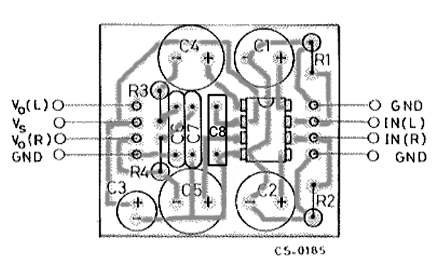
Note: The above image is copied directly from the datasheet and is not mine, nor is it likely to be 1:1 scale. To achieve this scale, the best idea is to print to PDF file to A4 paper. You could then use that template to drill and etch a PCB using cheap and simple techniques in my PCB building guide.
Reducing gain
Because the chip is intended for low output sources such as radios and cassette heads from those days, the schematic in the datasheet and shown above has a maximum gain of 39dB. That's a voltage gain of at least 89!
If your source is a phone, laptop, or portable player you'll find this gain too high and turning the volume control even beyond a quarter or halfway puts the sound into a distortion. Whilst reducing the gain won't increase the overall volume before distortion, it can improve the sensitivity of the volume and also reduce hiss/noise from the high gain. Lower gain improves the signal to noise ratio.
The schematic diagram on page 2 of the datasheet shows that the TDA2822M has internal resistors that are in the feedback. These are R1 and R2 for one channel and R5 and R4 for the second channel. The values for these internal resistors (based on a search!) are apparently 50k and 500 ohms respectively. This looks right as it gives a gain of 101 (40dB) - calculated as 1+(R1/R2) = 1+(50000/500) = 101. The (typical) gain the datasheet quotes of 39dB will include loses.
A more sensible gain to aim for is 26dB to 32dB (20x to 40x). To achieve this, we can add an additional resistor in to the feedback loop in series with internal resistors R2 and R5.
The voltage gain with the additional resistor can now be calculated as 1+(R1/(R2+Rext)), where Rext is our additional resistor. With an added 680 resistor in series, we get a gain of 1+(50000/(500+680)) = 43.3. In decibels this is 20*log(40) giving 32.7dB. 680 ohms is a common E12 value, but if you can get E24 resistors then 750 ohms will get your gain to 41. An even lower gain of 20 is little trickier but 2.2k (a common value) will give 19.5x (25.8dB), or 2k for 21x (26.4dB). Do not reduce gain less than 20x or the amplifier will oscillate.
These additional resistors should be 1% metal film or better so that the gain is closely matched for both channels, especially if you are adding high values.
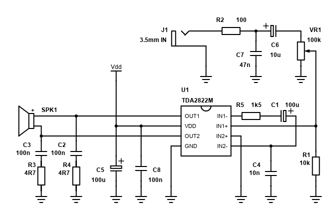
Below is the modified schematic, with the additional resistors R7 and R8.
| # | Type | Quantity |
|---|---|---|
| U1 | TDA2822M | 1 |
| U1 | (optional) 8 pin DIL DIP socket | 1 |
| R1,R2 | 10k ohm Resistor, ¼W Metal Film, 1% | 2 |
| R3,R4 | 4.7 ohm Resistor, ¼W Carbon, 5% | 2 |
| R7,R8 | Calculate, or 680 ohm Resistor, ¼W Metal Film, 1% | 2 |
| C1,C2,C3 | 100µF Capacitor, 16V+ Electrolytic | 3 |
| C4,C5 | 470µF Capacitor, 16V+ Electrolytic | 2 |
| C6,C7,C8 | 100nF (0.1µF) Capacitor, 50V+ Ceramic X7R or MLCC | 3 |
| VR1 | 100k ohm Dual Log Potentiometer | 1 |
| Vin L/R,+Vs,Spk L/R | 2.54mm header 7-pin (cut as needed) | 1 |
| Cable, connectors | ~ |
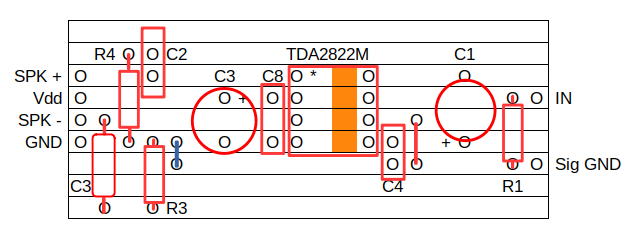
The stripboard layout for such configuration is also below. It's hardly any larger or more complex than the standard application and gives you flexibility with the gain. Even if you end up requiring the maximum gain, you can install jumpers for R7 and R9 to get to the maximum gain.
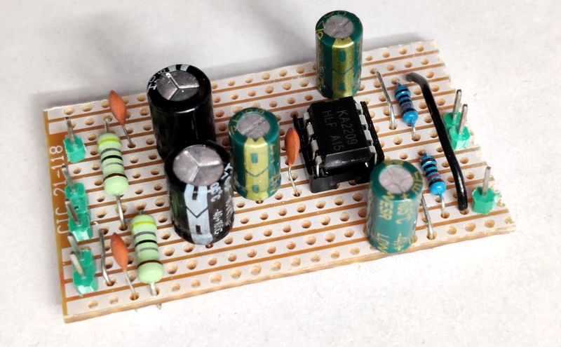
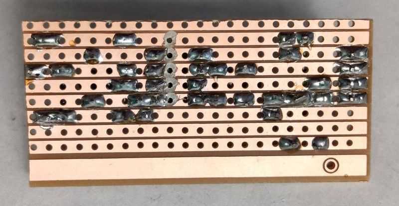
This is the version I have actually built and tested at the default maximum gain by using wires/jumpers for R7/R8 (as pictured) and with 680 ohm resistors to reduce the gain. It works well with no hum, little hiss and good stability. Below is a picture of my version (with KA2209 chip in it):
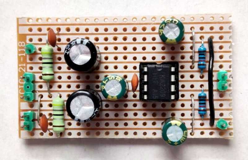
Note that the 4.7 ohm resistors are ½W types as it's what I have. As the TDA2822M is quite a low power amplifier though you could use ¼W resistors. The output capacitors I used are 470µF.
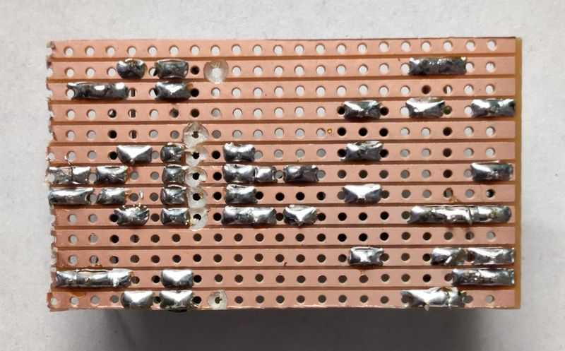
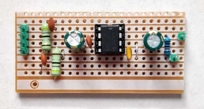
This picture below shows the underside. Soldered stripboard doesn't look nice, but it's quick to build and the joints work reliably with no shorts between the tracks. You can also see the track cuttings that I've made.
Bass boost
By adding a further capacitor and resistor (per channel) into the feedback loop in parallel with the internal resistor, we can add a bass boost to the TDA2822M / KA2209 circuit without any external boost circuit required. A bass boost may help your small speakers sound bigger than they really are but do note that it'll be at a cost of reduced volume output before distorting.
| # | Type | Quantity |
|---|---|---|
| U1 | TDA2822M | 1 |
| U1 | (optional) 8 pin DIL DIP socket | 1 |
| R1,R2 | 10k ohm Resistor, ¼W Metal Film, 1% | 2 |
| R3,R4 | 4.7 ohm Resistor, ¼W Carbon, 5% | 2 |
| R7,R8 | 100 ohm Resistor, ¼W Metal Film, 1% | 2 |
| R9,R10 | 3.3k ohm Resistor, ¼W Metal Film, 1% | 2 |
| C1,C2,C3 | 100µF Capacitor, 16V+ Electrolytic | 3 |
| C4,C5 | 470µF Capacitor, 16V+ Electrolytic | 2 |
| C6,C7,C8 | 100nF (0.1µF) Capacitor, 50V+ Ceramic X7R or MLCC | 3 |
| C13,C14 | 220nF (0.22µF) Capacitor, 50V+ Polyester or Mylar | 3 |
| VR1 | 100k ohm Dual Log Potentiometer | 1 |
| Vin L/R,+Vs,Spk L/R | 2.54mm header 7-pin (cut as needed) | 1 |
| Cable, connectors | ~ |
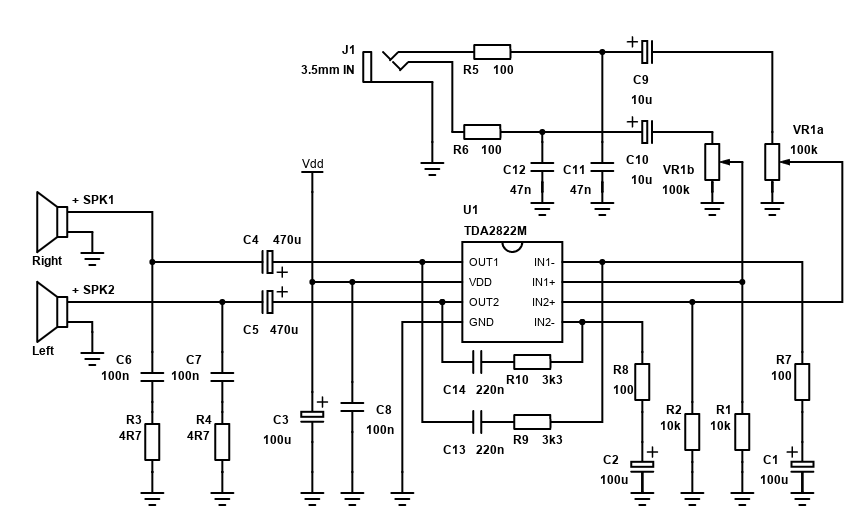
Not only has R7 and R8 been added (from above), but also a feedback loops from the speaker outputs to the inverting inputs. These are R9+C13 and R10+C14.
How this works (using channel 1 as an example) is high frequencies will pass through C13 and R9 from OUT1 back to the inverting input IN1. Compared to the 50k internal resistor on the feedback path, the value of R9 is much smaller at 3k3, so high frequencies mostly pass through the path of least resistance.
Low frequencies are blocked by the capacitor C13. This means they will mostly only pass only through the 50k internal resistor in the TDA2822M (internal R1), therefore bass frequencies will almost get the full gain (though the inclusion of R7 will lower that a little).
Using the values shown (3k3 for R9/R10, 100R for R7/R8 and 220nF for C13/C14), the neutral gain is around 27.5dB (24.5x). At 100Hz, it's 33.7dB (48.8x). Power gain is half the difference, so it'll be 3dB - twice as loud. At 55Hz the gain will peak at 34.2dB (51.5x) as the 470µF capacitors (C4/C5) in series with the speakers will start to roll off the bass frequencies. That can be considered a 'good' thing otherwise the gain will continue to climb until it reaches the maximum of 38.5dB (it's not 40dB due to the 100 ohm R7/R8). Many speakers will be so ineffective below 60Hz that the power lost there is a waste.
The values I've given is for a fairly large boost. To reduce the boost, actually you must increase the gain for the mid/treble frequencies. That means increasing the size of R9/R10. To compensate, increasing the value of R7/R8 beyond 100 ohms will reduce the mid/treble boost and the bass boost in line.
Altering the capacitors C13/C14 will affect the boost. Decreasing C13/C14 will result in both an increased gain at the same frequency as the larger capacitor as well as an increase of the gain bandwidth, as the impedance of the smaller capacitor is higher for lower frequencies, resulting in less negative feedback in the amplifier and therefore more gain. Increasing C13/C14 will reduce the gain and bandwidth to lower frequencies. Larger speakers should perform better with a larger value of C13/C14 as they'll get less bass boost, and restrict the boost to lower frequencies where they may still need it.
I suggest you prototype first on breadboard and try different resistor/capacitor combinations until you get a sound that's right for you and your speakers!
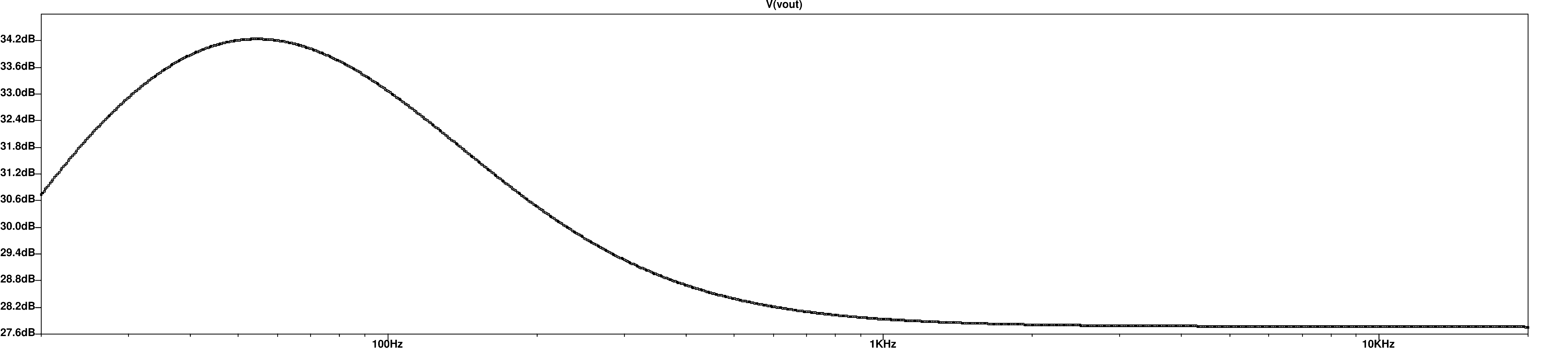
Here's what the gain will look like across the frequencies for the values I've suggested. The boost is from 250Hz and below as this is where small speakers will start to roll off.
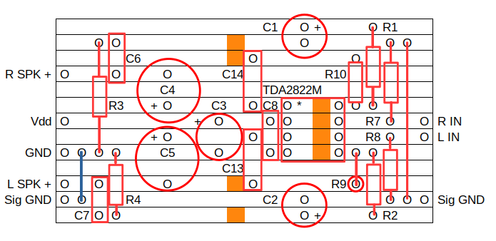
Below is a stripboard layout for the bass boost circuit. All these additional resistors (R7, R8, R9 and R10) must be 1% metal film. Capacitors C13/C14 should be some polyester or mylar film capacitors. At a pinch, ceramics will work, but they tend to reduce capacitance significantly when a voltage is through them so you may need increase the value to 1.5 or 2 times my suggestion.
You can 'defeat' the boost by shorting out the capacitors C13 and C14 with a DPST or DPDT switch, but this would need to be placed as close as possible to the TDA2822M as long wires to a defeat switch will cause the chip to oscillate.
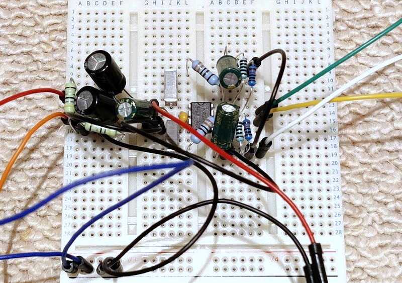
I've built this circuit on breadboard, and it works fine and sounds clear with a noticeable increase in bass. Because there is only 650mW available in the 6V PSU / 4 ohm speaker test scenario I used, distortion kicked in sooner, but there was still enough power for it to go loud and clear in a small room and I prefer the fuller sound compared to no bass boost. Feel free to experiment though and adjust the values of R9/R10 and R7/R8 in order to get the gains at low and mid/high frequencies correct for your speakers and max volume needs.
Power
The default gain of the TDA2822M is high, 39dB give or take. This means to drive it to its maximum power you only need a small signal, and no pre-amplifier is needed. This makes it ideal for plugging into portable devices such as the headphone output of music players, mobile phones etc.
To be a bit more precise, off 9V the TDA2822M provides 800mW of power into 8 ohms before noticeably distorting. To calculate the voltage of this, it's V = √(0.8 * 8) = 2.53V RMS. Divide that by 89 and it's just a 28mV RMS input signal required to drive the chip to maximum power, without distortion. A phone/smartphone or any portable music player that can drive headphones will easily give ten times this input power, so that's why I recommend reducing the gain.
The power output will depend on your configuration. For standard 8 ohm speakers, you can give a 9V power input to the TDA2822M in its normal stereo (non-bridged) configuration. That will give around 1W at 10% total harmonic distortion (THD), however 10% will sound really bad so really don't expect to push it much beyond 0.8W (800mW) at acceptable distortion levels. This means quite sensitive speakers will be required.
Into 4 ohms, you shouldn't go above 6V power input. The power output into 4 ohms at 6V is about 650mW, but at 10% distortion. In bridge mode, only 8 ohm speakers are allowed (because they'll look like 4 ohms to the bridged amp), and again 6V is the maximum power supply recommended. Bridged configuration gets you about 1.3W power into 8 ohms from 6V (at 10% distortion.
I have accidentally used 12V to supply a bridged TDA2822M and whilst it worked for a while, it eventually was permanently damaged, and the sound was distorted at all volumes - so bear in mind that the chip isn't invincible! With heatsinks and a ventilated case (unlike my closed speaker cases) it might survive at 9V, but it's a risk you'll take.
When using the chip at its maximum input voltage, I suggest a small DIP heatsink to allow heat dissipation, otherwise there is a chance of overheating with permanent damage when pushed.
While this amplifier is mainly intended as a battery-operated device, it can be used with DC power supplies too, and there are plenty easily obtainable that you can use, such as a 5V, 6V or 9V PSU. Universal DC adapters let you choose the voltage, and you should be looking at 500mA (minimum) to 1A or better current output so that the power supply is able to let the amplifier pull the power it needs to reach maximum power output to the speakers. Powering from a USB port is also possible.
Building a 'system'
Extra (simple) parts you may want to add to the schematic could be:
- 3.5mm jack input socket
- A power switch
- A power LED indicator
- Batteries
- 2.1mm power plug (for external PSU) - if wired correctly, this should disconnect the batteries when a plug is pushed into the socket
Bridge/BTL Version
There is a bridge schematic for this chip available in the datasheet. It is smaller still then the stereo version of the chip and it provides four times the power output into the same speaker load at the same voltage i.e., 1.5W into 8 ohms with a 6V power supply vs 380mW into 8 ohms with 6V for the stereo version. That's great - it allows us to use lower voltage power supplies/less batteries.
The amplifier will now be a mono amplifier though. If you want a stereo bridge amplifier you need two TDA2822M chips and repeat the schematic below.
That sounds worse, but because the components are fewer, including no need for output DC blocking capacitors (C4/C5 in the single ended schematic above), you'll save on some cost and room and two complete bridged TDA2822M amplifier will not take up much more space nor cost much more than a single TDA2822M in single ended stereo configuration. The component count is only slightly higher 23 for two BTL amplifiers (2 x 11 + 1 dual potentiometer) vs 16 and the PCB will not be much bigger.
| # | Type | Quantity |
|---|---|---|
| U1 | TDA2822M | 1 |
| U1 | (optional) 8 pin DIL DIP socket | 1 |
| R1 | 10k ohm Resistor, ¼W Metal Film, 1% | 1 |
| R3,R4 | 4.7 ohm Resistor, ¼W Carbon, 5% | 2 |
| C1,C5 | 100µF Capacitor, 16V+ Electrolytic | 2 |
| C2,C3,C8 | 100nF (0.1µF) Capacitor, 50V+ Ceramic X7R or MLCC | 3 |
| C4 | 10nF (0.01µF) Capacitor, Polyester or Mylar | 1 |
| VR1 | 100k ohm Log Potentiometer | 1 |
| Vin L/R,+Vs,Spk L/R | 2.54mm header 6-pin (cut as needed) | 1 |
| Cable, connectors | ~ |
Again, this circuit is as per the datasheet, with additional VR1 volume control, C6 DC blocking capacitor and R2/C7 low pass filter. The schematic is for a mono amplifier now - only one channel, so just duplicate everything for stereo. Like the stereo non-bridged configuration, VR1 can be a dual gang potentiometer to allow volume control for both amplifiers.
Resistors, again, should ideally be 1% metal film, but 5% is also fine. All capacitors are electrolytic capacitors except for C2, C3, C8 (100nF) and C4 (10nF) which should be ceramic capacitors. Because the maximum value of the capacitors is only 100µF, the cost of the components will be cheaper vs the non-bridged stereo version.
Below is my stripboard layout for the BTL circuit above. As can be seen, it's smaller and simpler than the stereo single ended version, but if you still want a stereo amplifier, you'll need to duplicate the whole layout with an additional TDA2822M chip.
I have built this stripboard version which works well and was simple to construct (taking just over 30 minutes to complete). Again, it works well with no hum, little hiss and good stability. Below is a picture of my version (with KA2209 chip in it):
This picture shows the underside. Again, soldered stripboard doesn't look nice, but it's quick to build and the joints work reliably with no shorts between the tracks. You can also see the track cuttings that I've made (including one unnecessary one).
The datasheet also has a PCB design, which as you can see is smaller than the stereo configuration. This sort of illustrates the point I made that having two BTL TDA2822M circuits won't end up much larger than the stereo version alone. Again, because of the image quality in the datasheet I've quickly edited it to make it a little clearer.
The gain for the BTL version remains about the same as the single ended version - I actually measured 70x voltage gain, around 37dB but that was off a 4.25mV RMS input.
If you want to reduce the gain for the BTL version, an additional resistor in series with the connected inverting inputs can be used in the arrangement shown below (R5). This 1k5 resistor cuts the gain to around 40x - that's 32dB. I measured 36x (31dB) on my test. This is a much more usable gain in my opinion and recommended. To lower the gain further to around 26.2dB (20.4x), use a 3.9k ohm resistor.
| # | Type | Quantity |
|---|---|---|
| U1 | TDA2822M | 1 |
| U1 | (optional) 8 pin DIL DIP socket | 1 |
| R1 | 10k ohm Resistor, ¼W Metal Film, 1% | 1 |
| R3,R4 | 4.7 ohm Resistor, ¼W Carbon, 5% | 2 |
| R5 | 1.5k ohm Resistor, ¼W Metal Film, 1% | 1 |
| C1,C5 | 100µF Capacitor, 16V+ Electrolytic | 2 |
| C2,C3,C8 | 100nF (0.1µF) Capacitor, 50V+ Ceramic X7R or MLCC | 3 |
| C4 | 10nF (0.01µF) Capacitor, Polyester or Mylar | 1 |
| VR1 | 100k ohm Log Potentiometer | 1 |
| Vin L/R,+Vs,Spk L/R | 2.54mm header 6-pin (cut as needed) | 1 |
| Cable, connectors | ~ |
The BTL version can drive 8 ohm and even 4 ohm speakers - which is impressive for such a small and simple amplifier! Keep in mind though that it is a small amplifier chip with no heatsink so you should not expect it to go beyond 2W of output power. This means if you are driving an 8 ohm speaker, the supply voltage should be around 6V to 7.5V maximum. For driving a 4 ohm speaker, 4.5V to 5V should be considered the maximum supply voltage. This makes the BTL version a great USB powered amplifier into 4 ohm speakers as it should get quite close to 1.5W of power output from 5V.
I don't recommend trying the bass boost trick above in the BTL version. Each amplifier half will need to be closely matched in order to share the load equally, but capacitors are rarely closely matched (usually a tolerance of 20%) and this will cause a gain imbalance between the two amp halves. The extra power from the bridge version does lend itself to having more headroom for bass boosting, so I instead recommend you do the boost with a passive or active bass boost circuit before the input.
That's about all that can be said about this amp because so many applications are possible from it. Both the TDA2822M / KA2209 / D2822A are all very cheap, and still quite available despite now being discontinued. If you want that little extra power, using a TDA7052 or TDA7052A is simpler, if you can find it! The TDA7266 is better still if your power supply is 6V or more and this chip is still produced so is a good recommendation.
TDA2822 application
The TDA2822 is also common in 90's radio cassettes
Quick facts TDA2822
- Power output stereo: 1.7W into 4 ohms at 10% 1kHz distortion with power supply 9V
- Power output stereo: 0.65W into 4 ohms at 10% 1kHz distortion with power supply 6V
- Power output stereo: 1.8W into 8 ohms at 10% 1kHz distortion with power supply 12V
- Power output bridged: 3.3W into 8 ohms at 10% 1kHz distortion with power supply 9V
- Gain: 39dB with standard application, can be adjusted down to 20dB with additional feedback resistors
- Power supply: 1.8V to 15V single supply
- Datasheet available here
Guide
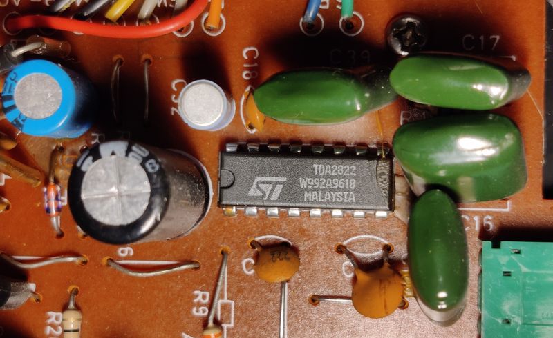
This section is about the TDA2822 16-pin DIP chip specifically (by ST), which is quite long obsolete now but I've seen it in at least two radio-casette players from the 90's (one I still own, which is made by Philips, choosing to use this ST chip instead of their own IC amplifiers).
All the advice above is very relevant as the chip has the exact same internal schematic diagram and configuration. The only differences are:
- Pinout: 16-pin DIP chip instead of 8-pin
- Higher power output: can be pushed to run 4 ohm speakers with 9V supply, 8 ohm speakers with 15V supply, or bridged into 4 ohms with 4.5V supply.
To achieve the higher power output, a heatsink should be attached per the datasheet example or a large copper area in the PCB given. I think finding the kind of heatsinks that fit is rare now, but it would do the best job compared to a copper area on the PCB.
You can use all of the schematics above with this chip, but you'll need to remap the pins per the table below.
| TDA2822M 8-pin DIP pin | Function | TDA2822 16-pin DIP pin |
|---|---|---|
| 1 | Output (1) | 6 |
| 2 | Supply voltage | 8 |
| 3 | Output (2) | 11 |
| 4 | Ground | 4, 5, 12, 13 (connect all 4 pins) |
| 5 | Input - (2) | 14 |
| 6 | Input + (2) | 16 |
| 7 | Input + (1) | 1 |
| 8 | Input - (1) | 3 |
Pins 2, 7, 9, 10 and 15 are all N.C. - no connection (leave them unconnected).
The stripboard layouts above of course will not work with this chip, but should be simple enough to adjust.
If you have this chip or can easily get it, it should also provide you with a simple to build amplifier. The chip is rarer though, but should still be easy enough to obtain on auction sites, once you scroll past the TDA2822M listings.