
TDA1514/TDA2040 Surround Sound Amplifier - Mark 3 - Surround Sound Amplifier 2020 Remake
1 - Ideas and Design, 2 - PCBs, 3 - Amps, PSU and Grounding, 4 - Digital Control and Software, 5 - Results and Pictures
Part 2 - Building, PCBs
On this page...
As the requirements for my rebuild were greater than the original amp, quite a few new PCBs had to be built, and in the end only one existing PCB was actually reused. Here are some more details of each.
Pre-amplifier PCB
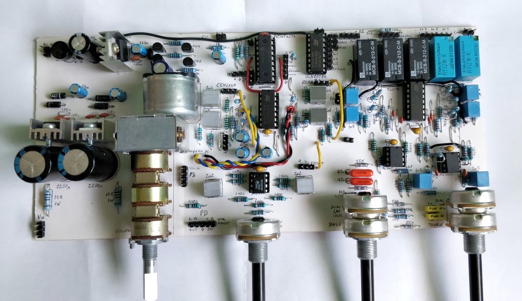
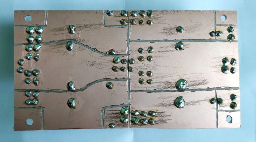
This is the main course of the meal! I think the most or second most complex PCB I've ever designed and built (as usual, all by hand).
It is tempting to use all the schematics and a computer program to produce a PCB layout which could be sent to a company to build a professional looking PCB for me. This may have taken less time, but I do prefer to go for the home-made approach. It's satisfying to know that my own effort went into the design, drilling, drawing, etching, and soldering of the whole board. There were a couple of constraints the board had to meet too.
The first constraint was that the holes for the controls already existed, so the controls (from left to right) for volume, balance, bass, and treble all had to sit in a specific location on the board so that they line up with the existing holes. The benefit is all these controls make a good mounting method for the board to float over both the surround decoder board and PSU.
The second constraint was that the board had to fit within maximum dimensions - so it is not protruding too far left and right of the controls and obstructing others, or too far back that it obstructs the PSU and amplifier boards. Copper PCB comes in a standard size of 100 x 220mm so that fit well without the need to do any cutting.
I then set about the design. The aim was to fit as much as possible on the board, but I could only guess what would actually be achieved so I started from the first constraint - the location of the controls, and then laid out components and traces on paper with pen and pencil. As I went, I kept the area as small as possible, for the size of my components.
On this board, I started with the ESP Project 97 Hifi Preamp which would control the front left/right channels. The tone controls are in the bottom right, so I started there and worked to the left where the volume control is, trying to go as little far up as possible.
Above that is a ground pour/bus which all preamps use. Then above that I laid out the 2x ESP Project 88 High Quality Audio Preamp (Mk II). This used TL074 quad op-amps to save space over dual ones.
Once that was laid out, there was just enough room for the input selection relays to sit at the top of the board on the right, so I placed those first and then saw that there would be just enough room to fit the ULN2003A array and PIC microprocessor too and it's input/outputs.
To the left of the microprocessor, and above the volume control, there was enough space for a simple H bridge to control the motor for the potentiometer.
I also had some space to the left of the volume control where a voltage regulator for the preamp chips (+/- 12V) and the microprocessor (+5V).
Despite the amount of circuits on one board, the only shame is that there still needed to be a vast number of headers connecting elsewhere. These are:
- 6 pin stereo inputs for the three input sources (leading to the relay switches)
- 2 pin switched pre-out leading to the surround decoder
- 2 pin decoder board input for Rear Left/Right
- 4 pin optional Rear Left/Right and Centre/Sub pre-ins for an external decoder (future use)
- 4 pin leading to the front volume adjust control input, and back, since this control was on a separate board
- 2x2 pin header leading to 'Rear Adjust' and 'Rear Balance' controls also on the separate board
- 2x 1pin separate in/out for centre channel adjust control, which is off board.
- 3 pin front Left/Right preamp output (leads to TDA1514 amplifier)
- 3 pin rear Left/Right preamp output (leads to TDA2040 amplifier)
- 3 pin optional Centre/Sub outputs
- 3 pin Regulated +/- 12V plus ground header to lead to the decoder board
- 4 pin set of ground headers for the audio signal ground (connected to the bus)
- 3 pin header for switched off-board relays (Power, Mute, Bluetooth power)
- 2 pin header for +12V for these relays
- 3 pin header for LED indicators for active relay
- 3 pin header for rotary encoder
- 3 pin header for IR receiver
- 3 pin header for IE LED, and power switch
- 2 pin +5V header (leading to Bluetooth, and Standby/Mute/Power LED transistors)
- 2 pin digital ground header (leading to Bluetooth)
- 3 pin unregulated +/- and ground 16V input
- 2 pin AC 9V input
That is certainly a lot! You will see that many wires connect to it in the final pictures. It's hard to see how it could have been any less though. Had I been designing the amp from fresh, I would have preferred to have the preamps and decoder + adjustment controls on one board, instead of the controller. Had I given myself complete freedom though, I probably would have used PGA2310 volume control chips and given it a display like my main amp, but the aim wasn't to make a clone of that, it was to do something different and learn a little more along the way!
The board design worked. It wasn't a perfect etch, because some air bubbles prevented some copper being removed where it was needed, meaning I had to leave it in longer than expected. Because of some scratches to the etch resistant pen too, some traces got hair width copper removed, which are easily fixed by bridging with solder, but still it would have cost me less time to avoid that in the first place.
There was also some mistakes and adjustments made after the build:
- Additional 5V outputs needed
- ICSP did not work - due to MCLR resistor and no diode to isolate the PIC from the rest of the circuit. I removed the MCLR resistor and configured the PIC to treat MCLR as input anyway
- Relay LED pins - I thought to use the 12V outputs of the ULN2003A, but these are floating when off, and ground when on but I needed the reverse, so I added a new header to 5V PIC outputs
- RA4 output for volume h bridge - RA4 is an open drain output on the PIC and it needs pull-up resistor
- IR pins were labelled incorrectly (flip +5V/In pins)
- More analogue ground headers were needed to solve hum when testing
- On the Project 97 tone controls, I connected R117/R118 into the - input of U2B, causing the tone control to have no effect. I wanted the full range anyway so removed these resistors.
For a hand-designed and hand-made board though - that's pretty good. Especially when there are more than 100 components on there. Designing the board took more than a day, building another day, and soldering it the most part of a day after!
Since 80% of the design is from ESP circuits, I won't provide details of the PCB - and given the effort if you were going for a new build especially, I think it's just worth buying the PCBs off that site directly. Having done so previously, they are particularly excellent quality.
The PIC microprocessor circuit
This is partially my own design, and it's quite simple for a controller.
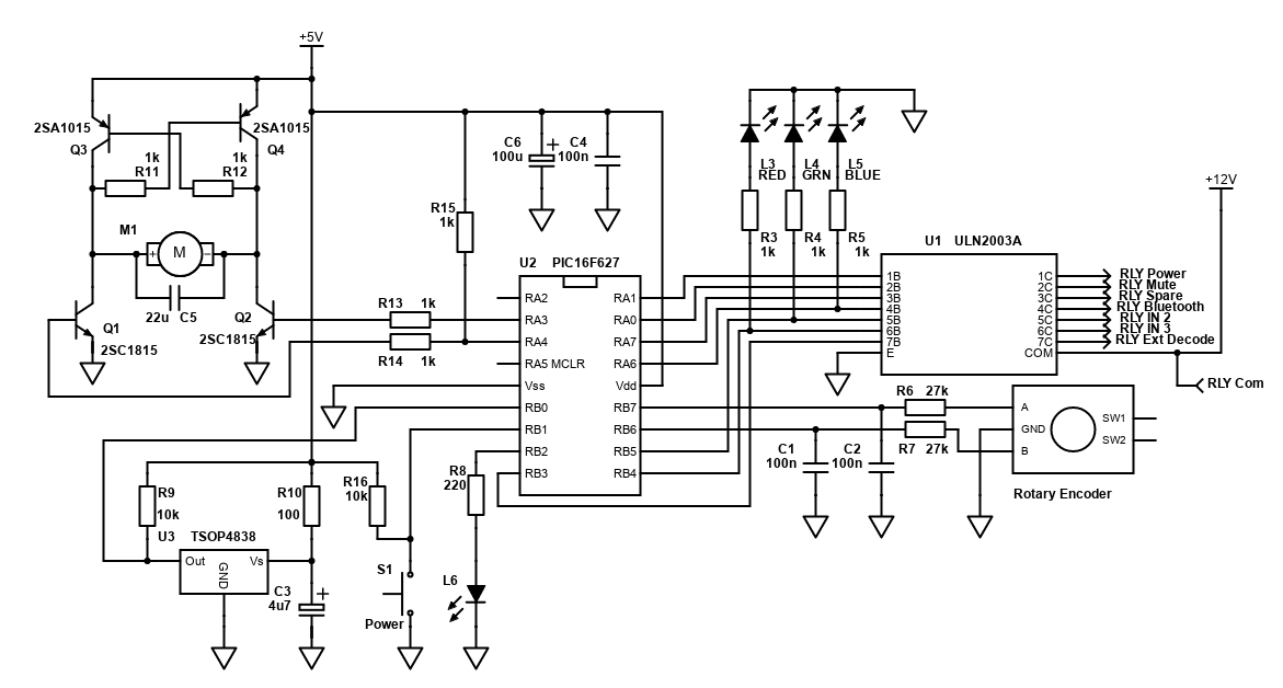
In the top left is a motor H-bridge circuit. This is a common circuit with designs everywhere. Given the motor current is low, I left off the back EMF protection diodes and used a simpler circuit requiring only two inputs rather than four.
The important thing about this design is ensuring the PIC microprocessor when coded never switches both inputs on at once. This would kill the transistors.
Output on RA4 makes the motor go forward (volume up). Output on RA3 makes it go backwards (volume down).
On the right is a ULN2003A. This is a 7-transistor array which includes protection diodes in a handy DIP package. It's perfect for taking the logic level outputs from the PIC (RA0, RA1, RA6, RA7, RB3, RB4 and RB5) and drive relays directly.
A rotary encoder is also present for the input selection, and a momentary push to make switch for the power.
Headers and pull up resistor for the IR sensor are present too (the IR sensor itself is off the main board).
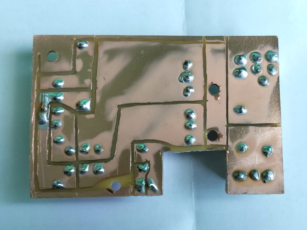
Surround Decoder PCB
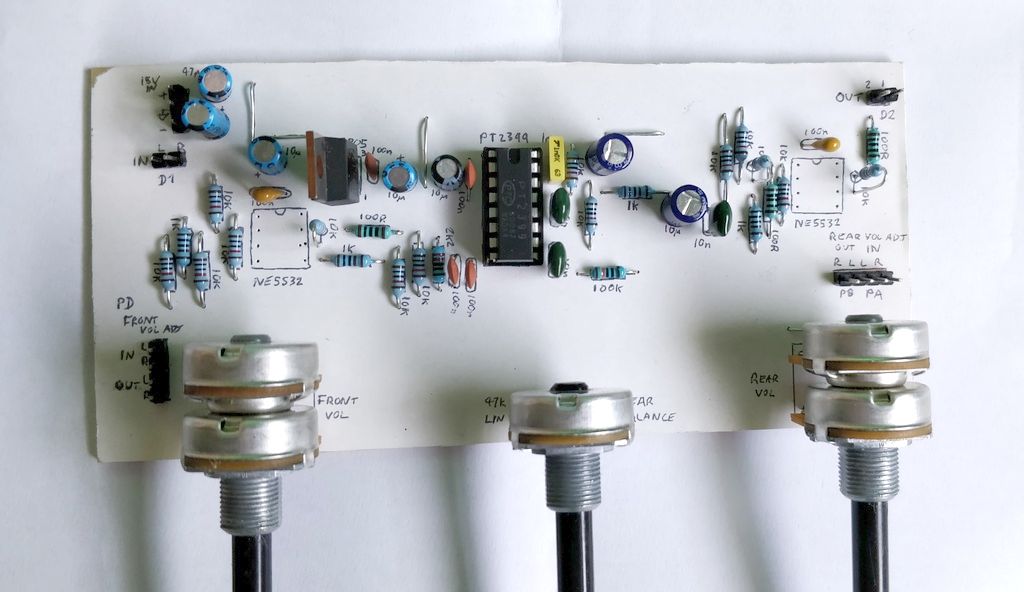
This board is a smaller board, and mostly consists of the surround sound decoder, as well as a mount for three potentiometers (front adjust, rear balance, and rear adjust).
The surround sound decoder uses the updated version on the ESP site, ESP Project 188 Surround Sound Decoder (Mk. II), but it sounds pretty much the same as the original, with the only extra benefit being that one of the rear channels is inverted, which produces a better effect.
Designing this board was much easier, again I started with the constraint of where the three potentiometers must be placed in order to align with the existing holes in the front of the amp. Headers to connect these to the main preamp board could then be placed, and in the space above that I managed to fit the Project 188 decoder, including PT2399 delay and the +5V regulator for that, all on the same board.
Still, because this board is separate from the main PCB, there were a number of headers - but not so much!
- 2 pin stereo left/right signal input (line level)
- 2 pin rear left/right Output
- 3 pin power +/-12V including ground
- 4 pin header to connect the front volume adjustment
- 4 pin header for the rear volume adjustment and balance *
* You may wonder why I just didn't make these follow directly after the decoder, well, this volume/balance adjustment should be after the first stage of the preamp per the design, which is on the main board, plus it is also there to adjust the level of an external decoder if used later.
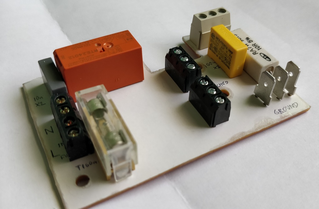
PSU PCB
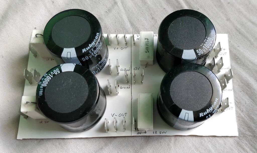
Strictly this doesn't need to be a PCB, but those snap in capacitors I have are easier to solder on a PCB plus I wanted to use spade connectors to connect/disconnect inputs and outputs from this board, which because especially important when experimenting with grounding.
This PCB is built differently. Because the copper needs to be wide (as low resistance as possible), rather than use lots of ink from my etch resist pen and then etch the remaining, I instead used a cutting disk to grind away boundaries for the traces.
The PCB is quicker to build in this way if the layout is simple!
Essentially, two power supplies are on this one board. Both consist of 10,000uF capacitors. One on each rail, so 2 per PSU, 4 in total on the board.
To reduce ripple a little further, 1 ohm resistors are also included in series with the input and the capacitor. This also forms an RC filter, giving a low pass filter of 16 Hz (below our hearing).
Instead of the small 2.54mm headers for Dupont connectors like the rest of the PCBs, I used PCB mounted spade connectors so I could use spade crimps on the power supply wires. These handle higher currents and have a lower resistance, which makes them better for PSU connections.
All in, there are quite a lot of spade connectors:
- PSU 1 - 2x DC 25V Input
- PSU 1 - 2x AC 0V Input for centre tap ground
- PSU 1 - 3x +25V Output (only 2 used)
- PSU 1 - 3x -25V Output (only 2 used)
- PSU 1 - 7x Ground (this is the star point for PSU 1)
- PSU 2 - 2x DC 17V Input
- PSU 2 - 2x AC 0V Input for centre tap ground
- PSU 2 - 3x +17V Output
- PSU 2 - 3x -17V Output
- PSU 2 - 7x Ground (this is the star point for PSU 2)
The DC inputs are from the bridge rectifiers, which then connect to the AC outputs of the transformers.
The AC 0V inputs are for the ground. Where the two transformer coils connect in series, this forms a centre tap, and it gives a ground reference for the amplifiers.
Later I'll clarify how these ground connections are made to all the circuits.
Mains board
There is a bit of mains connectivity to do. Mostly I needed a board to mount an AC switching relay, so that the main transformers could be safely switched on/off by the PIC microprocessor.
This board was also used for the capacitor and resistor in an earth loop breaker - something I usually include to remove hum when connected to an input device that is also grounded via the mains earth and causes a ground loop if so.
A fuse for the small 9V transformer was also mounted here, and screw down terminals for live in/out, neutral in/out and earth connections.
Since the layout is simple, I again took the small cutting disk to the PCB to make a layout but was a bit more generous with the width of the gap because these are mains voltages involved.
Once complete, this board was also insulated with spray on PCB lacquer. Not a guarantee of safety, just a little more protection.
LEDs and IR sensor board
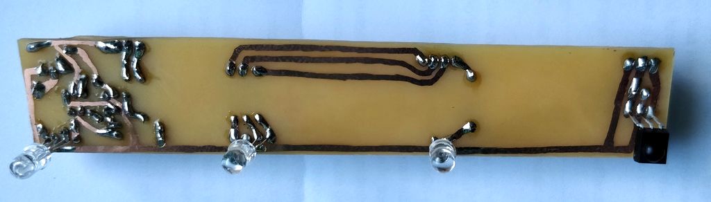
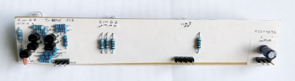
This board was for mounting the LEDs, with some transistors to control them, and also a mount point for the IR sensor.
Three holes for 5mm LEDs were already in the case front so I designed this board to align with those, plus drilled another for the IR sensor.
The three LEDs are:
- An RGB LED for power status where red = standby, green = muted, blue = on
- An RGB LED for the active inputs where blue = input 1 (Bluetooth), green = input 2, red = input 3
- A blue LED for IR activity. This just blinks as visual feedback that the remote-control commands are being read
Interfacing the RGB LEDs required some work. Both RGB LEDs are common cathode, so the common pin goes to ground.
The input one is simple enough and each colour would be activated whenever the relay for the input was activated, so by using the outputs of the PIC micro-controller (before the ULN2003A) with resistors in series
The power status LED was more work though. I didn't leave any spare ports on the PIC to control it, so I used a bunch of transistors to build a set of logic gates in order to make the below truth table:
| State | Power Relay | Unmute Relay | Red | Green | Blue |
|---|---|---|---|---|---|
| Standby | Off | Off | x | ||
| Muted | On | Off | x | ||
| Normal on (unmuted) | On | On | x |
And of course, if the whole unit is disconnected from the mains, all colours would be off.
The circuit to meet this logic is this:
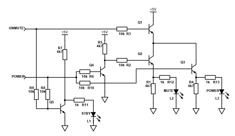
In the 'Standby' condition (red LED), both relay inputs are off (pulled to 0V by the PIC).
Q5 is a NOR gate (Not OR). When a voltage is present on either (or both) inputs, the transistor switches on, shorting the LED to ground so it is off. When both inputs are off, the current flows through the LED instead, causing it to light up.
The 'Mute' (green) LED needs to be on only when the power relay is on. It must be off when the power and unmute relays are both on, and off when both are off.
This logic is a bit more complex, but can be done with an AND gate, and an Inverter. Q1 and Q2 form the AND gate. Current will flow through the collector to emitter of these two transistors only when a current is present on both of their base pins. Q1 is connected to the Power connection directly, but Q2 should be ON only when the Mute connection is off. Q4 is an inverter. When a current is applied to the base, the transistor pulls the collector output to ground, so ON becomes OFF and likewise OFF becomes ON.
Finally, the 'Power' (blue) LED should only be ON if both the power and unmute relays are ON. This is an AND gate, this time without the Inverter. Q1 and Q3 form this AND gate. To save on the components and make the PCB layout easier, Q1 is a shared for the mute and power AND gates.
This is all small signal logic, so the choice of transistor is not critical. They are all NPN transistors and I used 2SC1943 ones because I have them. Those are really old transistors though and BC549 or anything from BC546 to BC550, 2N2222 or similar is what you'd choose. Check the pinout as they vary!
An alternative to the transistor approach would be to use a 1-of-4 binary decoder, such as the 4555 (i.e. HCF4555B, CD4555B). This has two decoders in it, so one can be ignored (by grounding the inputs). For the used decoder, Q0 would be the standby LED as it's true when both inputs are false. Q1 would be for mute, assuming the input B was connected to the power on signal. Q3 would be the power on condition, because both inputs A and B are now true.
Bluetooth module mount
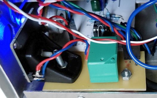
This was added right at the end to mount a relay allowing the Bluetooth module to be powered on/off. The reason for this is because the Bluetooth module has no password to connect to it and since I live in a flat I did not want it active 24x7 and it only activates now when the amplifier is powered on and the Input 1 is selected.
References and more reading:
The Audio Pages - Elliott Sound Products
HyperPhysics - Transistor logic gate examples
RoboRemo - Simple H Bridge with 4 transistors