
7.1 channel Hi-Fi microprocessor/PC controlled Preamp
I suggest reading about the rebuild first. Information below is for reference purposes.
Inputs/Outputs
I decided from the start that I would make this a 7.1 channel preamp. This means when (or more likely, if) 7.1 surround sound becomes common all I would need to do was add an extra stereo amplifier and rear speakers. Since the cost to have those additional 2 channels (as opposed to 5.1) would be small compared to the overall cost.
So, for inputs and outputs I would need an 8-channel output, and an 8-channel input. For the rest of my equipment, I would include an extra 5 stereo inputs, which would be decoded into a simple Hafler Matrix surround sound using an simple decoder, and appling the mono rear output to all 4 rears (or 2 as current) and a centre output to the centre channel and subwoofer.
All the inputs and outputs are switched using DPDT relays, and muted using 4-pole relays too, in order to prevent the nasty pop the preamp would otherwise make if you turned it on after the power amp. These relays are controlled via a Darlington transistor array, such as the ULN2003A, and then a shift register such as the 74HCT595 in order to reduce the 7 I/O pins to a more managable 3 pin serial connection.
Analogue flow/connections
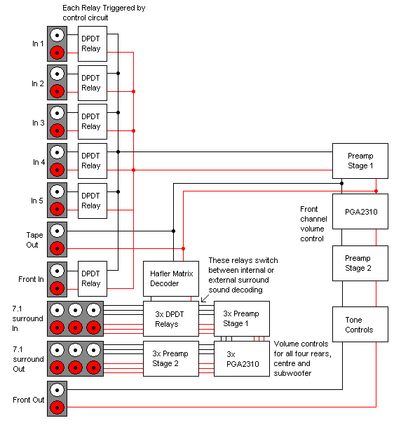
To get the best idea of the layout of this preamp, it is best to look at the analogue connections first. I have produced a diagram that shows the flow of audio from each input to each output.
Analogue Flow and connections
At the time I drew this diagram up, I hadn't added the muting relays - they were an idea I thought I had better implement after I built the revision one board and realised there was quite a nasty pop on power on and off. The phono preamp was added later too, and this goes in between In5 and its relay.
The PGA2310 is the digital volume control which with 4 of them, allows the microchip to control all individual 8 channels seperatly, or together. In my current setup, I am able to change the volume to every channel (like normal), but also able to cut/boost volume levels to rear, centre or the subwoofer channel. Balance is also possible, but un-implemented at this time because I consider it un-necessary.
The halfer-matrix decoder mentioned in the diagram is Project 18 from ESP. It can only provide mono rears, but with 80% of music, this is actually a very nice effect as long as the rear remains a little quiter than the main speakers. It also provide the correct effect for a centre speaker and a subwoofer (the subwoofer needs an additional low pass crossover, which is not provided in my preamp).
Preamp stage 1, PGA2310 and preamp stage 2 boxes refer to the circuit on the previous page showing the main audio path.
Relay connections - digital
ULN2003A
Most relays operate on 12 volts DC. Even the ones that do operate on 5V draw too much current for them to be directly connected to the PIC I/O pins or standard logic outputs.
I added a 7812 regulator to my power supply to handle the relay voltage - but how would I simplify driving the relays from 5V logic?
Well, this is really simple when you consider a simple NPN transistor switch (with back EMF protection diode) would work... but when I have over 10 relays to drive - this amount of transistor plus their base resistors and protection diodes etc means a complex and large PCB very quickly.
A cheaper and easier solution would be to use a Darlington array, such as the ULN2003A. This is like 7 transistor switches, with protection diodes, all in one DIP package.
However, currently for every relay there has to be a free port on the PIC to drive it. This is not acceptable as with at least 10 relay signals, 10 pins will be needed.
Shift Register - 74HCT595
This idea came from Mark's preamp, where he uses shift registers to control multiple data lines. He says this is well known, but it was the first time I saw it (although I have seen it more often now). It's a great idea, and perfect to reduce 14 I/O lines down to 6.
Shift registers themselves, are effectively a serial to parallel convertor. They have no internal clock and so are driven by the clock pulse sent from the PIC micro - making them ideal to use at a higher or lower clock speed than 4MHz. The other two signals are the data (0 or 1 for that output 0-7) and the latch - used to output the configuration in the internal register onto the chips parallel output, meaning that as I send serial data, the parallel output won't change until I latch it. Neat eh?
Although an 8-bit serial byte is sent to the shift register, and there are 8 outputs, the LSB (least significant bit) is not used. This is because the ULN2003A only supports seven relays, so I left off the awkwardly placed Q0 pin on the shift register floating.
This put my bit usage for relays A and B as follows:
Relays A
- Trigger 4
- Trigger 3
- Trigger 2
- Trigger 1
- Sub/Centre mode select
- Mains Out Switching
- Rear mode select
Relays B
- CD (In 1)
- Tape (In 2)
- Tuner (In 3)
- Phono (ln 4)
- Aux (In 5)
- PC/DVD (In 6/Front In)
- (NOT)Mute (for all channels)
In my code, this list is actually reversed because I send out the data LSB first, meaning that bit 7 is unused, not 0. This is my fault - it wasn't clear from the datasheet whether it should be MSB first or LSB first, so I used LSB first and used some code to see which relays would be affected from each change. MSB first is the right way to do it, but I didn't make any changes... if it ain't broke, don't fix it :)
C2C Code for the relays
|
This fragment of code is what I use to send a byte out to the shift registers, and then latch it so the bits set in that byte cause the relays connected to the shift registers' parallel output to switch on.
There is an important global variable here - relaysB (or relaysA for the first routine if you have another shift register like I). This variable is set by other parts of the program - in my case the serial receive routine which reads the relaysA variable sent from PIC #1.
Connections in the above routine are all on port b. Pin 5 is serial Data (DS/SER), pin 6 is Clock (SH_CP/SRCLK) and pin 7 is Latch (ST_CP/RCLK). They can be changed as you see fit.