TDA1514A DIY Guide - 50W High Performance Hi-Fi Amplifier
Warning: This chip has long been discontinued and if sold and cheap - it will be fake! If you're buying, make sure it is from a good supplier (i.e., not auction sites) to get the genuine chip otherwise performance will be bad, the chip may be easily damaged and create a hazard, or hum/buzz may be worse than the official chip. Due to the lack of availability, even though it's a great sounding chip, I can't recommend it for new builds. The LM3875/LM3886 chips are the next step up and also sound great.
Recommended Experience : intermediate, knowledge of amplifiers, split rail power supplies, PCB etching, heatsink attaching, and mains qualification
TDA1514A application
Quick facts
- Power output: 51W into 8 ohms at 10% 1kHz distortion with power supply +/-27.5V
- Power output: 40W into 8 ohms at 0.1% 1kHz distortion with power supply +/-27.5V
- Power output: 28W into 8 ohms at 0.1% 1kHz distortion with power supply +/-23V
- Power output: 48W into 4 ohms at 0.1% 1kHz distortion with power supply +/-23V
- Gain: 30dB using datasheet components (adjustable 20 to 46 dB)
- Power supply: +/-10V to +/-30V dual supply only
- Datasheet available here
Guide
Of many single chip hi-fi amplifiers, the TDA1514 (TDA1514A) is one of the best single chip amplifiers that you will find which was good value and good performance in its day. It has many applications. None are suggested by the data sheet, but the main application is obviously Hi-Fi (signed for use with Compact Disk Digital Audio). Here are some of my own ideas for this amplifier:
- Stereo Hi-fi amplifier
- Small subwoofer amplifier
- TV amplifier
- Surround Sound Amplifier
- PC speaker improvements, or other such speakers with built in amplifiers
- For hi end projects this amp may also be used for mid-range or tweeter amplifiers in bi/tri amplifier systems.
The TDA1514 / TDA1514A or NTE7118 are 9-pin single in line (SIL) chips with 2.54mm (0.1in) spacing. The chip has slots either side which should be used to mount it to a big heatsink (with insulating washers). There is also the compatible NTE7118, but this is also hard to find, and I've never tested it.
With the datasheet application circuit, it doesn't really require many more additional components and all of those are easily available. The design is for a split rail power supply.
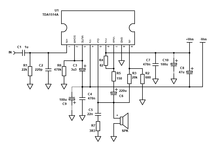
The circuit above is a re-drawn copy of the same one found in the Philips TDA1514A datasheet, found here. This chip is now long discontinued and the only two I brought and made were purchased from UK Maplin around 2002 and the chip was already discontinued shortly after I put this website up. This information page is just for reference now for those who manage to get hold of the chip.
Despite me building it successfully at the age of 19, it's more complex than most of the amplifiers I feature on this site, and I wouldn't recommend it as a first build. Those builds still work today though, and if you do find it working and attempt it, it's a very pleasing amplifier!
- Great Value
- High Power
- Low distortion (harmonic and distortion)
- Thermal Protection
- Doesn't click when switching on and off
- Sound quality is excellent.
- Up to 50W of power!
If you are building this amp for lower powered applications (it will run on PSU's right down to +/-10V), then this chip will drop straight into a stripboard PCB with no awkward bending of pins and such, and other components should be accommodated with ease. If you do attempt this, ensure bypass capacitors C4, C7 and C6 and feedback resistors R3, R2 are close to the chip and use a Stripboard track cutter to break the excess length of strips where no more components or jumpers are required.
I wouldn't recommend stripboard when powering this amp at over +/-17V (from a 12V transformer) and in these cases where you do want the extra power from this amplifier, please design your own PCB with thicker tracks to handle the power better due to lower track resistance. I designed my own board, and it works well despite not knowing much about PCB design at the time. Even though more components are involved, the final board size is still quite small.
Components and Construction
All resistors are recommended to be 1% metal film, recommended for the accuracy of their values. The 3.3 ohm resistor R6 should be rated 1W.
Capacitors should be electrolytic with values exceeding 1µF. Most electrolytic capacitors should be rated at 50V minimum and must be connected the right way round! The 47µF electrolytic C8 must be rated 63V or better as it lies between the positive and negative supply rails. With +/-25V supply, that's over 50V flowing through that capacitor.
The 1µF input capacitor C1 should be polyester type for best performance. With 1µF the cut off frequency is 8Hz which is fine for bass extension, but you can go higher if you wish.
The 0.47µF (470nF) bypass capacitors C4 and C7 should be ceramic (or multilayer ceramic MLCC) and placed close to the IC pins, as should the 22nF Zobel capacitor C5 and 220pF RF frequency filter capacitor C2.
The supply bypass capacitors are quite small. My build still works well, but the lead length to the PSU board in my build is pretty short though so if you feel more comfortable, you can consider adding 100µF electrolytic capacitors in parallel with C4 and C7 (I've drawn C9 and C10 in the schematic), rated 35V minimum, 50V ideally.
![]() Note: The datasheet recommends that bootstrap components should be altered when using 4 ohm speakers. R4 change from 82 ohms
to 47 ohms and R5 change from 150 ohms to 82 ohms. Otherwise for 8 ohm loads, leave them as the recommended values. I don't
recommend you use 16 ohm loads and absolutely never use 2 ohm loads (including 2x 4 ohm speakers in parallel).
Note: The datasheet recommends that bootstrap components should be altered when using 4 ohm speakers. R4 change from 82 ohms
to 47 ohms and R5 change from 150 ohms to 82 ohms. Otherwise for 8 ohm loads, leave them as the recommended values. I don't
recommend you use 16 ohm loads and absolutely never use 2 ohm loads (including 2x 4 ohm speakers in parallel).
A critical part of the construction is that the TDA1514 chip must be put in the board the correct way round! The side with a metal square is the back - this is the part mounted to the heatsink, therefore the side with the part number printed on it is the front and pin 1 is on the left.
It is critical that you get a damn good heatsink! These devices do warm up quite a bit when pushed hard, without a heatsink, they would overheat almost immediately. Make sure your PCB design leaves space for a large heatsink, and therefore I recommend that the TDA1514A chip is located at the edge of the board so it can be fixed to a heatsink easily without the board protruding into the heatsink area.
The chip must also be isolated from the heatsink using mica washers or Kapton tape otherwise the metal back, which is connected to -V (not ground) will short with the heatsink, which in most applications is likely to be grounded - your case and heatsink must be earthed in a DIY build. Before turning on, check with a multimeter that resistance is high between the -V supply rail and the heatsink. If it is low or full continuity, then check you've isolated the chip from the heatsink correctly.
The gain using the components per datasheet is 30dB. That's a good value and how mine is configured. If you wish to change this though, the values of R2 and R3 determine this where the voltage gain is 1 + (R3/R2) e.g., for R2 of 680 ohm and R3 of 20k ohm: 1 + (20000/680) = 30.41. In dB this is 20*log(30.41) (assuming an input voltage of 1V RMS) which equals 29.66dB. Do not go configure these for a gain lower than 20dB, or higher than 46dB - if you need such a high gain, I recommend a pre-amp for better performance.
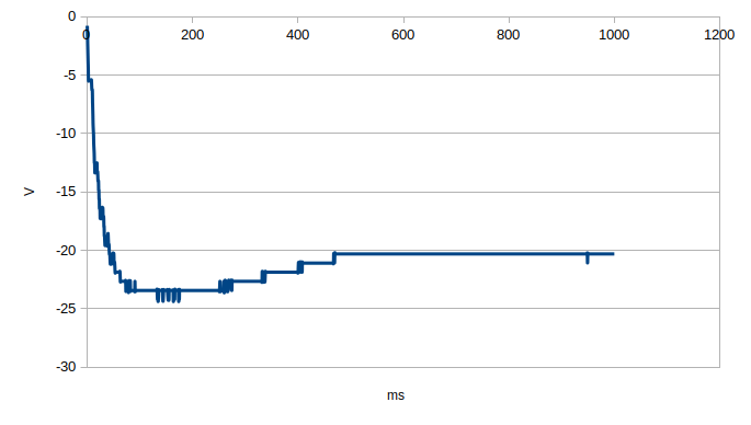
The TDA1514 contains Mute and Standby (pin 3). The above schematic from the datasheet application will use the pin properly with C3 providing a short time delay to before un-muting the amp as it is charged from -VS to -VS − 6V (maximum allowed difference is 7.25V) - this is a technique to reduce power on/off pops through the speaker. The difference between -VS (pin 4) and the mute pin determines the state. On my system, pin 3 settled to -20.3V in about 460ms, which is about 6V higher than the -VS rail.
Standby - with no difference between pin 3 and 4 (i.e., mute pin = -VS) to 0.9V difference puts the amplifier in standby state - quiescent current is low in this state and the amplifier is fully off. Current is still not as low as switching off the power entirely, but I can imagine TVs or similar equipment of the day using this feature.
With a difference of 2V to 4.5V, the amplifier is in mute. The output gets switched on here, but no (or very little) input signal will get through to the output. A difference beyond 6V puts the chip in an operating state.
I've plotted the voltage measured during power on below. You might note that it looks less than 5V difference, but the power supply rail would have continued charging as C3 charged.
I recommend you don't adjust the muting circuit design anyway. I use separate relays for speaker muting as they can also be used for speaker protection in case of failure. Whilst the TDA1514 has been reliable for many years, you should always protect speakers, especially if they are expensive. See ESP Project 33 Loudspeaker Protection and Muting for a suitable design.
PCB
Since the datasheet does not contain a layout, here are a few designs, and my original hand drawn version too.
Updated 28/09/04
I have been kindly submitted PCB layouts from a reader named MC Mike. He has made drawings of his own layout and mine on PCB software and has allowed me to host them here for the benefit of others. This is recommended layout.
MC's original is here, and it is provided with the following information:
| R1 - 20k | C1 - 1µF |
| R2 - 680 ohms | C2 - 220pF |
| R3 [R6] - 470k | C3 - 3.3µF |
| R4 [R3] - 20k | C4 - 470nF |
| R5 [R7] - 3.3 ohms | C5 - 22nF |
| R6 [R5] - 150 ohms | C6 - 220µF |
| R7 [R4] - 82 ohms | C7 - 470nF |
| C8 - 47µF |
The components are slightly renamed, I've put in brackets the designator from my schematic above.
My original design - with more reasonable component placement widths
These designs above may help out those who can make boards with more specialised equipment and may also be clearer for the humble etch resist pen user like me. Both should work fine, but the first design is probably the better choice but as the TDA1514 is not available anymore, I won't be able to build a new one and verify the design works fine, but the principles look good.
Below is my original hand-drawn layout, which is verified as working and free to use if you so wish. I designed it so many years ago I make no claims that the design is ideal though and I am also not responsible should it not work - the 470nF bypass capacitors should be closer to the chip for example. Despite this though, it does work well!
Tracks on the real board were drawn thicker than the pencil design, and I recommend you do the same for best performance. The image should be printed to a size of 12cm by 7.1cm. It is unlikely that the image below will come out at a 1:1 scale.
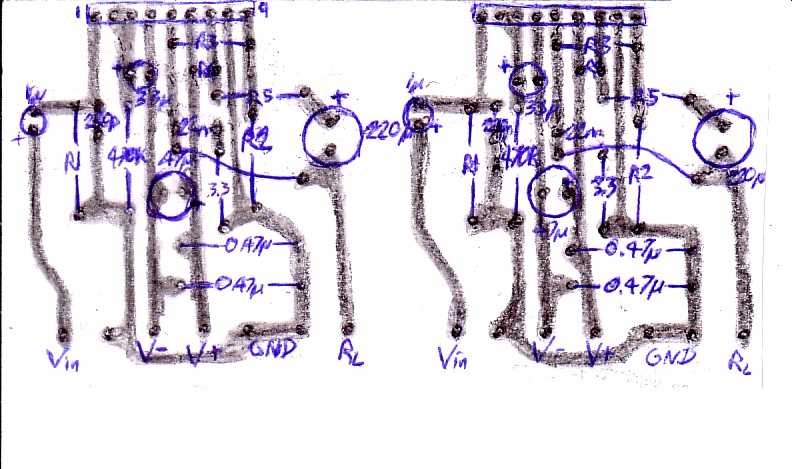
Usage of the PCB layouts is not critical. But do make sure you take the necessary pre-cautions. Make sure all capacitors go in the right way round and also the amplifier chip. Make sure that the tracks you draw on the board are accurate and as wide as they can be without getting too near other tracks (as this could cause a short circuit when the board is etched).
Note that the first two layouts are mono. Duplicate for stereo (you'll need two of everything, including the TDA1514A chip). My hand-drawn layout is for stereo - using two TDA1514 chips. The right amplifier is simply a copy of the left. The left amplifier also labels the pins 1 and 9 of the TDA1514 chip, make sure that these are correct, and the right is exactly the same way wound. The image of my finished amp below shows an illustration of this.
Performance
After wired correctly, the TDA1514 is a great amplifier, actually really great. Consider it Hi-Fi and will compete against quite a few commercial systems, and some well rated commercial amplifiers even use it (example Cambridge Audio A1).
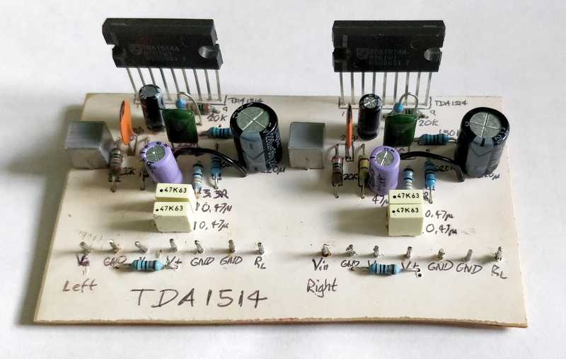
I use two of these amps in my surround sound system. They are my main amplifiers for the front channel, and I've used them with Mordaunt Short MS20i Pearl speakers, Mission M71i speakers and now JBL Control 1 speakers, and they've all worked great, particularly the Mission speakers. The power is in the region of 30 to 40W but it does open up very nicely and is capable of party volumes. Above is the picture of the two TDA1514A devices on my home made PCB.
The TDA2040 operates the other three channels, rear right, rear left and the centre. Sound from this system is very good indeed, more capable with movies then music, but still gives an enjoyable experience and it will be my main hi-fi system for some time to come I imagine. A fine collection of great chip amplifiers.
This amp will also suit many other purposes, I will leave you to use your imagination, but I do recommend it for its simplicity, cost and superb performance. I don't think many single chip amplifiers will rival it for cost and sound, though the LM1875 and the TDA2050 could be its main contenders of the time, and LM3875/LM3886 are (now old but still produced) more modern alternatives.
Power Supply
A power supply for this amp is simple. You need to wire up a 18-0-18 (or 2x 18V AC) transformer in order to get +/-25V which I recommend. You can read my article here for assistance wiring toroidal transformers. This involves mains wiring:
THE POWER SUPPLY REQUIRES MAINS VOLTAGE WIRING. DO NOT WIRE IT UNLESS YOU ARE SUITABLE QUALIFIED, DEATH OR SERIOUS INJURY MAY RESULT.
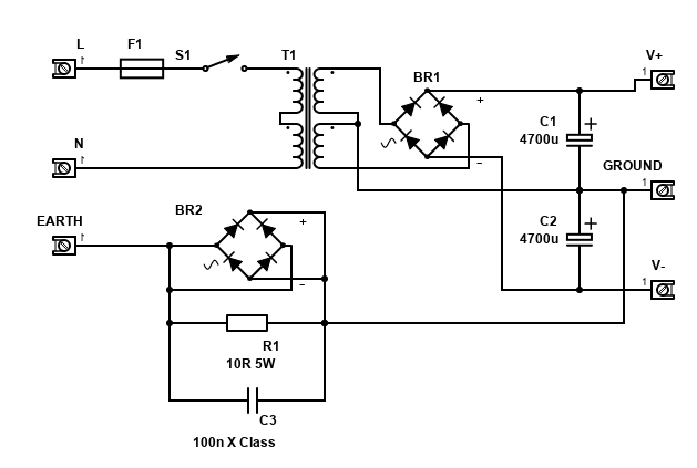
For one amp, a 60VA transformer for T1 should be sufficient, meaning if you have two amps, 120VA is the recommended, 80VA will drive two, but sustained power is likely to be affected. Capacitors should be 4,700µF or bigger, rated at 35V - I went for 10,000µF as this smooths the rails more effectively and also creates a reservoir for intermittent power draw. Feel free to increase the capacitance further but you may not get much additional benefit for the price involved. Do make sure they are connected the right way round too or they will be ruined, potentially exploding and causing injury.
A fuse should be installed (F1), I will leave it to you to work out what's appropriate because of the world-wide mains variations. The fuse must be a time delay (slow blow) variant (e.g., T250mA) if using toroidal transformers.
Be sure to correctly earth the supply and any metal casing around it and the amplifier.
The components on the earth and ground connections form a loop breaker. This is recommended construction because it can eliminate those evil earth loops. R1 is a 5W or better wire-wound resistor. The 100nF capacitor must be rated for 250V AC, you cannot use a 250V DC cap as it would fail if there ever was a fault causing mains to flow to earth. Check your country's rules and regulations before constructing this as it may be illegal. If so, omit all these components and connect the earth to ground but never disconnect the earth lead... it could save your life or somebody else's!
That covers most of the design, but please remember to read the datasheet (linked above).
