
ADAU1701 / ADAU1401 Audio DSP Information and Expansions
Introduction
The ADAU1701 and ADAU1401 DSP chips, also known as Sigma100, are 2nd generation DSP cores from Analog Devices. Although the chips themselves are now getting close to 20 years old, they still make a capable DSP audio solutions that can potentially replace lots of analogue line level circuits.
These chips include the ability to control volume, switch inputs and outputs, mix inputs, generate signals, do many different types of crossovers (at the exact frequencies you need), tone controls, parametric EQ, (short) delays, bass boost, room EQ (REQ) and much more.
The boards from China I now see sometimes as low as £12 to £14 including delivery. For me, that makes it an incredible value DSP... but you do have to bear in mind that if it's your first SigmaDSP then you do need to buy a programmer too. This bumps the cost somewhat more, but you can use it again to build more systems and change things later. I now own three of these DSP boards, plus an ADAU1466 and ADAU1452!
What makes the SigmaDSP chips good for me is SigmaStudio. Daunting at first, but it's a good compromise between ease of use and flexibility.
The ADAU1701 is also used in the WONDOM / Sure APM2 and JAB3, Dayton Audio DSPB-K and KABD amplifiers, 3e audio EDSP-1701-24-A.
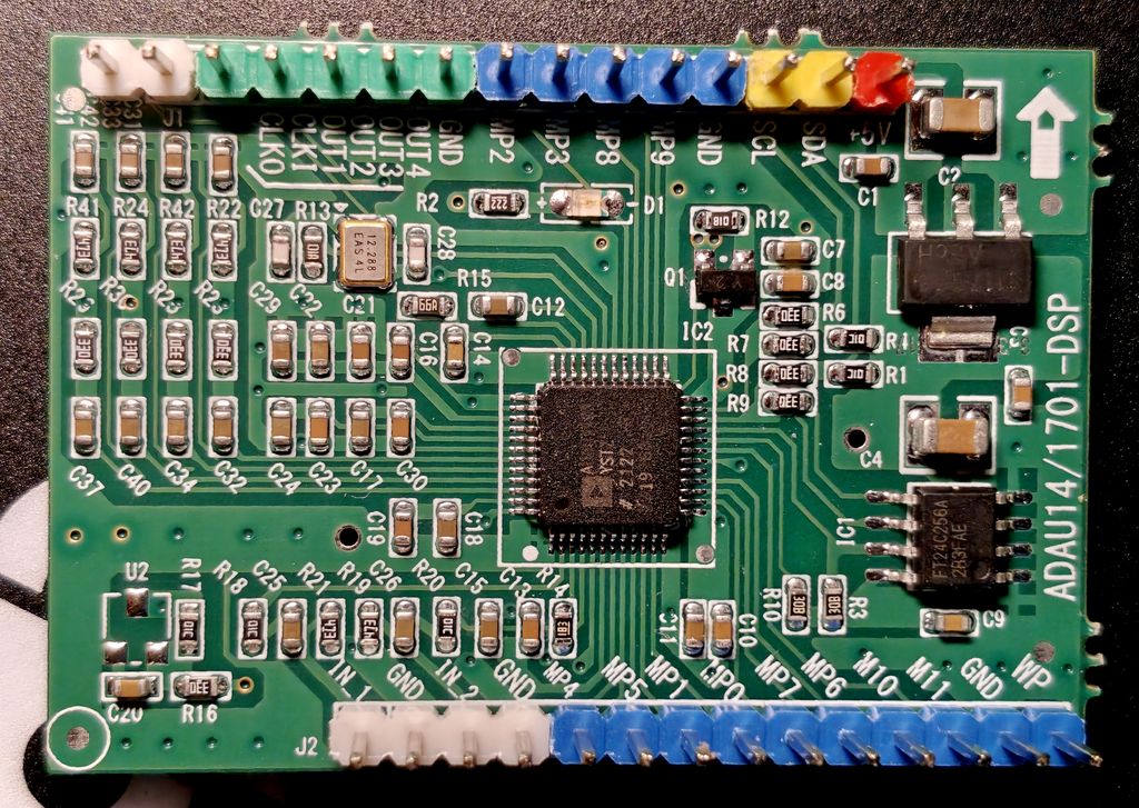
About the Boards
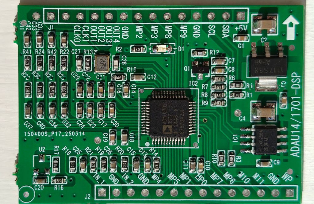
Anyway, what about these ADAU1401 / ADAU1701 boards? Some have the ADAU1401 and some have the ADU1701. There's no difference except the ADAU1401 can work under more temperature extremes and is automotive certified.
They include a single stereo analogue input (or two individual mono inputs if you like), and two stereo outputs (or four mono), because the DSP chip itself does. Unlike later SigmaDSP chips, there is no need for separate ADC and DAC chips. Both are 24-bit resolution converters. Inside the core, you have a 28-bit resolution. Sampling can also be up to 192 kHz. SNR and THD performance are also good.
I'd consider it Hi-Fi - perhaps not going to satisfy audiophiles but where it 'may' lose some quality of pure analogue circuits (that you'd unlikely to hear), you gain the ability to perform much more EQ and room correction so you can end up hearing detail through speakers that you may not have before.
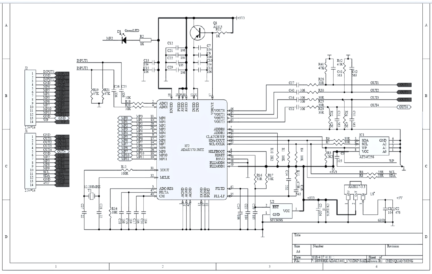
Below is the schematic. I can't find a good quality original, so this is upscaled a bit with upscaly and output curve adjusted. It's not great, but clearer than the original.
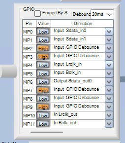
The DSP has 12 multipurpose I/O pins, labelled MP0 to MP11 (MP0 to M11 on the board). These allow you to connect button switches, rotary encoders and/or potentiometers to control things like volume, tone, input selection and more inside the DSP directly. For simple systems, this means no additional microcontroller is needed.
The multipurpose pins can also be digital outputs, so you can light LEDs or trigger relays, but since these pins can only drive 2mA - even an LED will need an external transistor or logic level MOSFET unless it's high brightness. A relay would probably need a Darlington or logic level MOSFET to drive it properly.
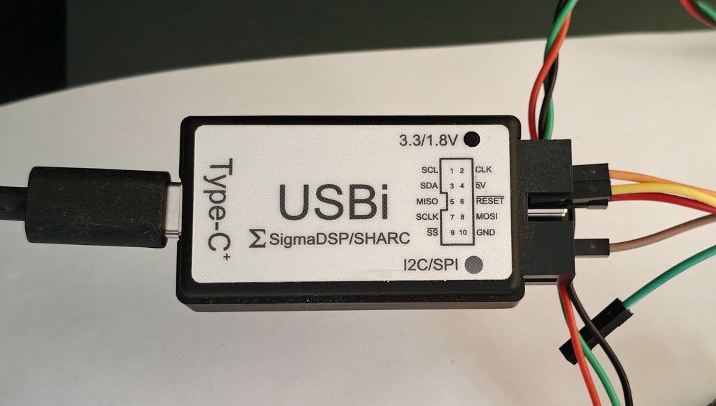
For programming, the board has an I2C header. The programmer I brought didn't have a compatible cable (these are extra), but a cable is easy to make with some cable and a DuPont connector kit and crimping tool.

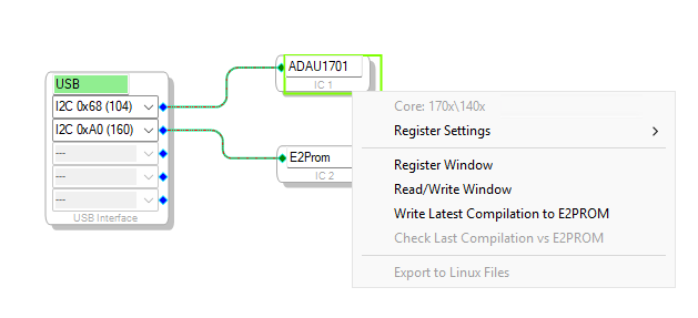
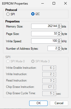
An external 256K EEPROM is also included (FT24C256A). This allows you to self-boot the DSP from a program stored here. To do this using an I2C programmer, ensure the EEPROM is connected to the DSP in SigmaStudio with address 0xA0. Place a jumper on the DSP header to bridge WP to GND (bottom right on the board picture above).
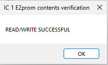
Use SigmaStudio to write the program to EEPROM "Write Latest Compilation to E2PROM", then confirm the write was successful by reading it "Check Latest Compilation vs E2PROM". You need to have run "Link, Compile, Download" at least once before these options are enabled. If it fails - check your jumper is set correctly.
Here are some other notes about the board:
- No headers are soldered usually. Standard 2.54mm headers fit fine.
- There are no mounting holes, and no place to even drill one. You might want to consider soldering unused pins to a piece of prototype board or a custom PCB, so that can be mounted separately.
- There's no overvoltage or reverse voltage protection.
- It pops at power on/off and when programming new DSP programs via SigmaStudio, so consider amplifier muting circuits during on/off and disconnect speakers when programming.
- There's only a basic passive filtering circuit on the output. I'd suggest only using short cables to your amplifiers.
- My board also doesn't have the STC803S supply-voltage monitor present. This looks like it resets the DSP under low voltage brownouts, but if your 5V supply voltage is stable, this shouldn't be required.
- The DSP board I have has a green LED connected to MP2. I guess it's high brightness since there is no driving transistor. I've used MP2 for a potentiometer driven ADC before on this board, and it would light the LED when the potentiometer is rotated to its minimum, so I recommend removing the LED from the board if you do this.
- If you need +3.3V, there is no output header for this, but you can solder a single pin into the hole next to C4. This gives +3.3V from the AMS1117 LDO regulator which is useful for external potentiometer connections or other uses.
- With 5V USB, I measured 70mA power consumption (340mW) including the programmer.
- There is no reverse voltage or over-voltage protection, although the AMS1117 will tolerate voltages up to 15V, power dissipation will become an issue. 6V is likely fine, 9V (400mW dissipation) is pushing it too much for my liking. A direct 12V connection means more than 600mW dissipation though and that will be quite hot for a small regulator that only has a small PCB as a heatsink. Use an external 7805 regulator if you have to do this or a buck convertor. An isolated DC-DC convertor is perhaps even better if the 12V (or other) supply is shared with an amplifier.
Furthermore, there are limits to the chip itself:
- Only 2 analogue inputs (1 if stereo) and 4 outputs (2 if stereo)
- I2S connections are tricky, especially inputs. There are no ASRCs (asynchronous sample rate converters).
- If you do make I2S connections, this reduces the amount of pins available for controls. For example, one I2S input and two I2S outputs will leave you with four remaining pins (conveniently though, those are the four ADC capable pins).
- It only allows 1024 core instructions per audio cycle for 48kHz. This halves to 512 core instructions for 96kHz and halves again to 256 instructions for 192kHz. Therefore, if you want the best sampling quality, you can only build a few filters and functionality before running out of available instructions.
- On this last point, it's not immediately clear if you go over the limit. The DSP just goes silent when you press "Link, Compile, Download". To find
out how many core instructions your dspproj used, look for a folder in the same location and inside there is a net_list_out2 folder and a
compiler_output.txt file.
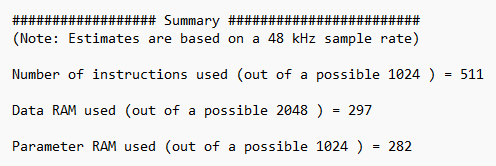
Example above shows my program just inside the limit for 96kHz, which will be half the limit shown (512)
As for the clock speed, for the DSP board described, this has a crystal of 12.288MHz feeding MCLKI. The PLL0 pin is grounded (0) and PLL1 pin is connected to +3.3V (1), so MCLKI is 256 × fS. The fS should be always set to 48kHz so the core is clocked correctly, i.e., 12.288MHz / 256 = 0.048MHz (48kHz). The core clock is 49.152 MIPS, which is MCLKI × 4.
Expanding via I2S / Serial Ports
This DSP supports I2S Inter-Integrated Circuit Sound (also known as IIS, I2S), TDM, Left/Right justified audio inputs and outputs, so you may think that gives you the freedom to connect many different digital inputs and outputs. That's often not true though - read below first!
| Pin | I2S Wire | Sigma Studio I/O |
|---|---|---|
| MP0 | Input Data 0 | Input channels 2, 3 (stereo) |
| MP1 | Input Data 1 | Input channels 4, 5 (stereo) |
| MP2 | Input Data 2 * | Input channels 6, 7 (stereo) |
| MP3 | Input Data 3 | Input channels 8, 9 (stereo) |
| MP4 | Input LRCLK | |
| MP5 | Input BCLK | |
| MP6 | Output Data 0 | Output DIG0, DIG1 (stereo) |
| MP7 | Output Data 1 | Output DIG2, DIG3 (stereo) |
| MP8 | Output Data 2 | Output DIG4, DIG5 (stereo) |
| MP9 | Output Data 3 | Output DIG6, DIG7 (stereo) |
| M10 | Output LRCLK | |
| M11 | Output BCLK |
* Caution: There is an LED connected to this pin so it may not work as an I2S input. Consider another pin, or removing the LED.
Via the multipurpose pins, I2S inputs and outputs are possible. However, here's where this board is limited - "The serial data clocks need to be synchronous with the ADAU1701 master clock input".
There are no ASRCs (asynchronous sample rate converters). This means the clocks must match up from the external board and this DSP. Practically, this limits things as most modules all are clocked from their own crystals for convenience and that's not a problem with most hardware.
There are ways to get things working though and that usually means having slave support for your modules or clocking them including the DSP from a single master clock (MCLK).
When testing I2S peripherals, keep your SigmaStudio program simple and start with 48kHz. Don't try and make your whole project with all the filters, mux's, volumes and so on until you've confirmed your modules work.
I2S Outputs - DACs, Amplifiers
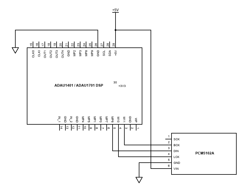
For DACs and amplifiers, it's likely to be easy because most DACs and amplifier chips run in slave mode. The DSP can be the master for these. PCM5102 is an example of a cheap and widely available DAC module that's actually good quality (Texas Instrument Burr-Brown). TDA7808 is an example of quad channel amplifier with 2 slave I2S data inputs.

The DSP I2S output would typically be set to master mode, and the following settings for 48kHz:
- Frame sync time: LRCLK
- Frame sync frequency: internal clock/1024 - 49.152MIPS / 1024 = 48kHz
- MSB position: delay by 1
- Word length: 24 bits
- BCLK frequency: internal clock/16 - 49.152MIPS / 16 = 3.072MHz, which itself is the frame sync frequency 48kHz * 64 (32 bits for each channel)
For 96kHz, adjust:
- Frame sync frequency: internal clock/512
- BCLK frequency: internal clock/8 (this gives 6.144MHz)
- Program Length needs to be at least 2 × (512 instructions)
For 192kHz, adjust:
- Frame sync frequency: internal clock/256
- BCLK frequency: internal clock/4 (this gives 12.288MHz)
- Program Length must be 4 × (1024 instructions)
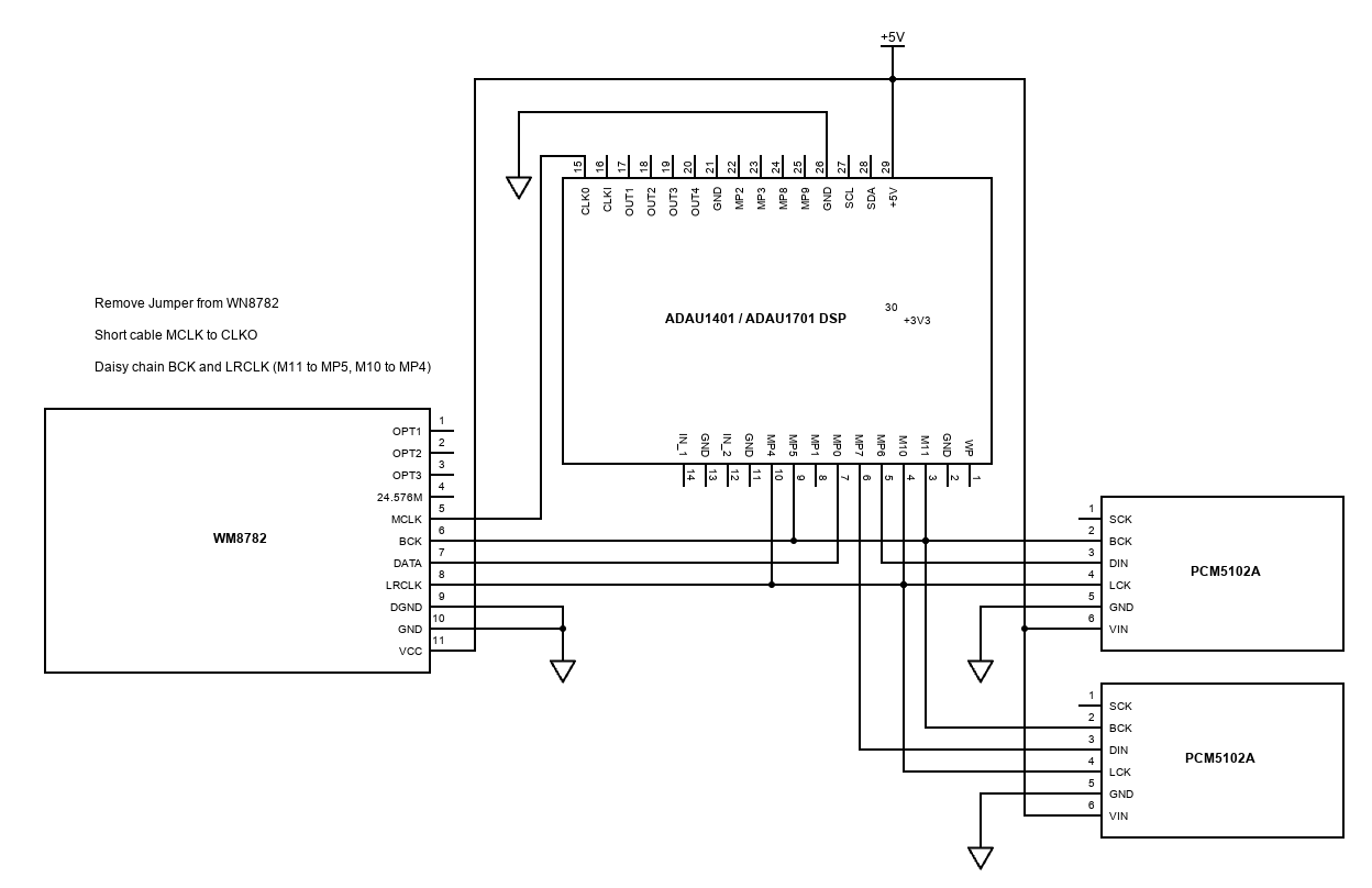
If the DAC or amplifier needs a master clock MCLK, the ADAU1401 board I have has a pin for this, but it won't be a square wave. You may need to buffer this unless that device clock in is a Schmitt trigger input and keep the wire as short as possible if used.
PCM5102 DAC
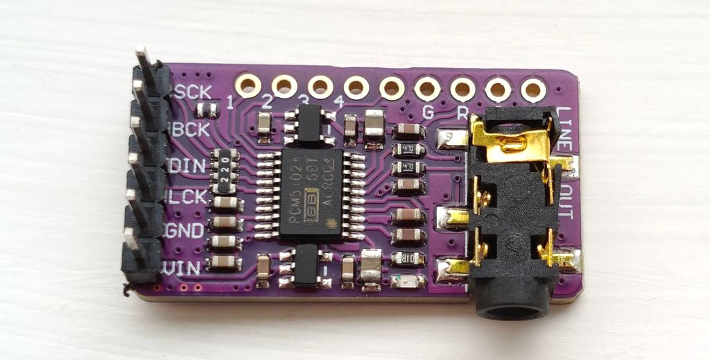
Status: Works well.
PCM5100, PCM5101 and PCM5102 DACs module boards can be found for very little, using PCM510xA chips from Texas Instruments.
These take I2S, Left-Justified signals and produce a stereo analog output and support a 3-wire I2S interface (without MCLK / SCLK). It will support 192kHz sample rates too.
The DAC runs in slave mode, so the I2S output of the DSP should be set to master.
Unless you're designing your own PCB with DSP and DAC close to each other, I wouldn't suggest supplying the MCLK to the DACs SCLK. This is high frequency, so layout and EMI are challenges.
Below is a schematic of how to connect the DAC:
TDA1543 DAC
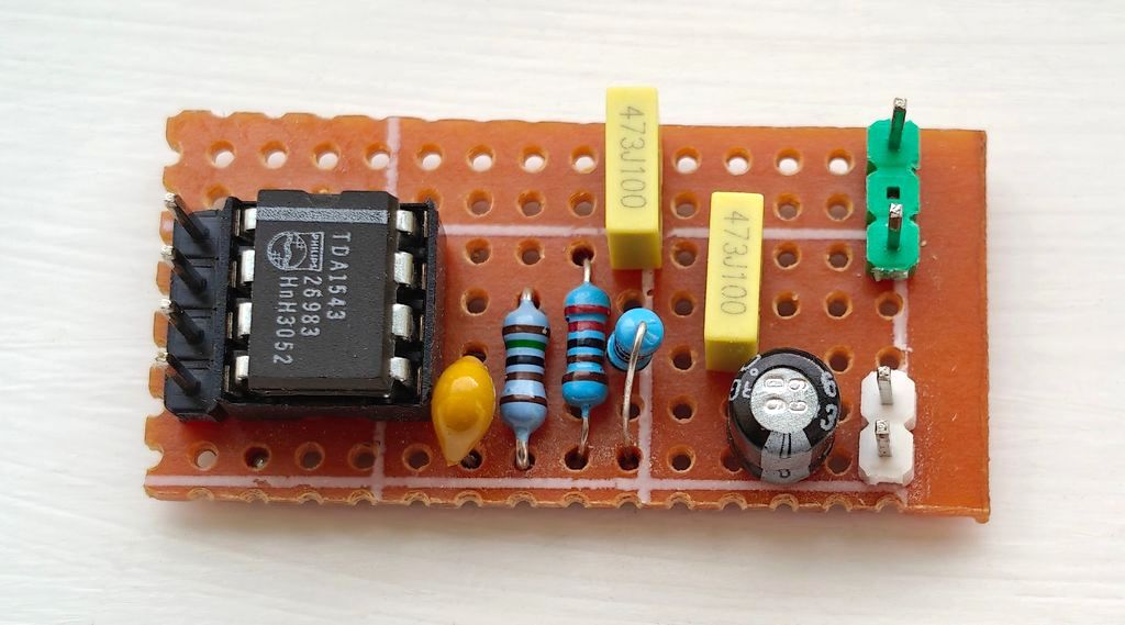
Status: Worked except at 192kHz.
TDA1543 is a vintage DAC I have, and I thought I would give it a try. It was highly praised back in the day when it ran in Hi-Fi CD players. Now, it is unlikely to outperform the above, but some may prefer its sound.
I made a stripboard version of the TDA1543 very quickly to test whether it would work, and it does so fine.
Mine ran fine with I2S at 48kHz and 96kHz, but not 192kHz. With a better power supply and proper layout though yours might.
I2S Inputs - ADCs, Bluetooth
For ADCs or other I2S inputs - it's a challenge. In fact, I've spent quite some time and money here so I'm writing down my experience, so you don't!

The I2S input on the ADAU1401/ADAU1701 is a slave only and typically I2S sources such as Bluetooth boards are masters. No problem you think, except the DSP is clocked via its own crystal oscillator, and this is unlikely to match the exact clock rate that the upstream master board is clocking audio bits out at.
It ends up in either nothing, a whine or a kind of robotic like distortion.
A solution can be to remove the crystal from the DSP board and supply the master clock from the input device - i.e., the Bluetooth board, ADC, TOSLINK convertor, etc.
The problem is that these boards typically only output the master clock when running. I brought a USB QCC3034 Bluetooth board and found it only generated a master clock once the phone was connected and playing audio. This limits the ability for the DSP to run otherwise, meaning you can't select another source.
Alternatively, order sources that support slave mode. The DSP can act as a master input by connecting the master BCLK and LRCLK output pins to the input, that is:
- MP11 to MP5 and then to the BCLK pin of the ADC/Bluetooth board
- MP10 to MP4 and then to the LRCLK pin of the ADC/Bluetooth board
- MP1 (or MP2, or MP3) is connected to data.
Below is an example of connecting a slave ADC, including the MCLK (you may not need this).
When making digital connections - keep leads as short as possible. Don't daisy chain grounds, and don't twist the cables together (i.e., do not twist the data with the BCLK / LRCLK and/or MCLK wires). Try running at 48kHz first before pushing sample speeds higher.
PCM1808 ADC
Status: Should have worked with this DSP but didn't.
This board is a pretty cheap module available online and can run at 48kHz or 96kHz rates. The benefit of this ADC is that it can be converted to a slave device by bridging some jumpers with solder.
This makes connectivity with the ADAU1701 easy as no removal of the crystal or connection of MCLK is needed.
Unfortunately, the PCM1808 just does not seem to send any audio out in slave mode. I captured what looks like healthy BCLK and LRCLK going into the PCM1808 fine, but DATA was just held low despite providing a signal.
In master mode, the PCM1808 works fine alone, but of course it is not aligned with the DSP clock, so no signal is read by the DSP.
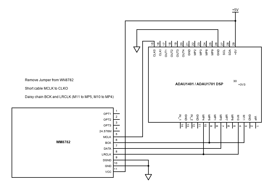
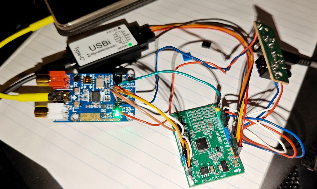
WM8782 ADC
Status: Works with MCLK
The Cirrus Logic WM8782 is another ADC online with slave selection support. Unlike the PCM1808, you don't need to solder anything, and moving one DIP switch is enough to make the ADC work in slave mode.
I got sound through the DSP at 48kHz, 96kHz and 192kHz I2S speeds, but there was also a clicking noise mostly on the right channel, regardless of speed. Powering the ADC off a separate PSU did not help either.
Perfect sound could be achieved by sending the DSP's clock out to the ADC though. I could test this because the board I have has a jumper that can be removed to disconnect its internal crystal, allowing MCLK to be supplied externally. With a short cable (10cm including connectors) from the DSP's CLKO pin (top right as pictured), 48kHz, 96kHz speeds worked perfectly. Sadly, 192kHz speed made loud white noise!
See the above section for how a schematic of how the WM8782 can be connected.
The downside is that the WM8782 ADC module is around the cost of the DSP board, so you could consider two DSP boards instead!
Qualcomm QCC3034 Bluetooth Module to I2S
Status: Not working with this DSP, but other modules may be programmable.
Early on in my investigation, I bought this board which looks like a high-quality module, with a USB audio input too so you can connect a PC to it directly and play audio directly.
Qualcomm Bluetooth boards are regarded as the best quality, but I had no luck with connecting it to the DSP. As a master, the non-synchronous clocks gave distorted audio.
Using Qualcomm software, it might be possible to reconfigure these Bluetooth boards as I2S slaves. In this mode, the bit clock and LR clock are sent from the DSP.
Now, there are various Qualcomm software version downloads from Chinese and Russian file shares! I did try using these to change the board settings and whilst I could get into debug mode, it appears the firmware on my one is locked, or I didn't find the correct software versions to be able to set anything more than the Bluetooth name and some other simple settings.
However, it should be programmable if you buy from a different seller. Search for "APP name change password Bluetooth QCC5124 QCC5125 QCC3034". A NoHFP board with noencrypt might be the best bet and then use the software linked to their google drive.
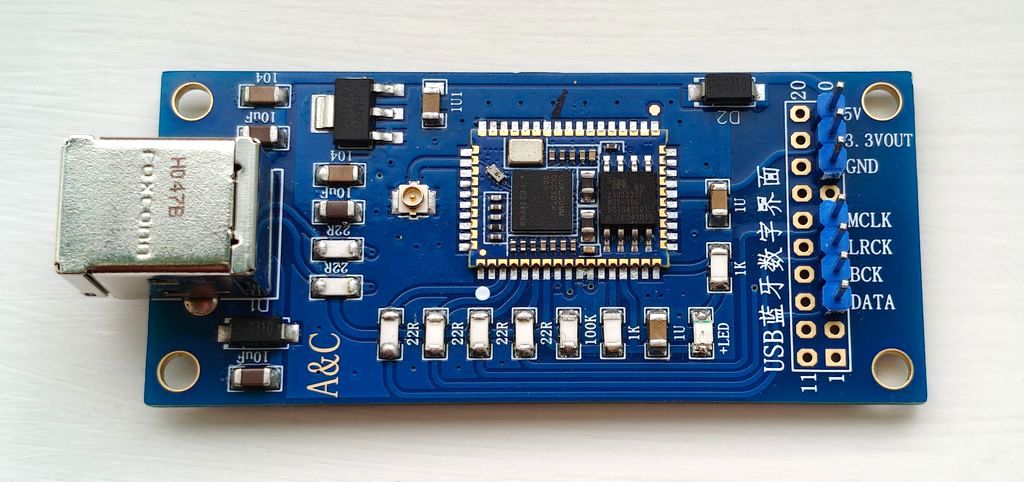
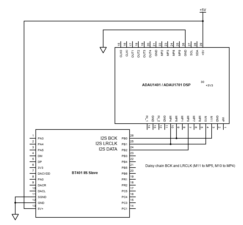
BT401 Bluetooth Module to I2S
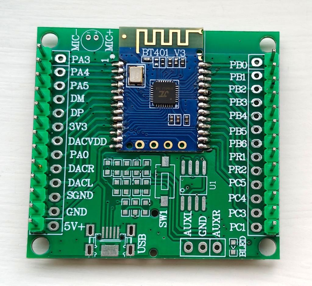
Status: Works at 48kHz (if the seller sends you the right one!)
I struggled to find Bluetooth modules that support I2S slave.
This cheap BT401 module does have the option though. You must specifically find a seller that allows you to order it as programmed as an I2S slave. It's unlikely to be Hi-Fi quality, but it sounds fine when connected as an audio only device.
Details about this module are thin. The datasheet and dfrobot site are of little use because it's for the common configuration rather than the I2S (IIS) option. I did find these Chinese links gave the most help: https://blog.csdn.net/qyvhome/article/details/109286938, https://blog.csdn.net/qyvhome/article/details/89320544.
The pins are 1.27mm spaced. The whole module is really tiny! I suggest ordering the bare board with it, so you can solder some normal 2.54mm headers to connect to. It does make the footprint of the solution almost six times larger though, but still small enough for most DIY projects.
Unfortunately, the first board I got was programmed as an I2S master and sends out the clocks.
I decided to try a different seller and the second time I was luckier. This module works perfectly with the DSP board but only seems to support 48kHz I2S. I think this is OK - that's still CD quality sound with no artifacts converting from analogue before and giving Bluetooth compression reduces some fidelity anyway; you are unlikely to gain much from a higher I2S bus speed.
Below is a schematic of how to connect to the DSP:
... and pictured working:

I2S Inputs and Outputs
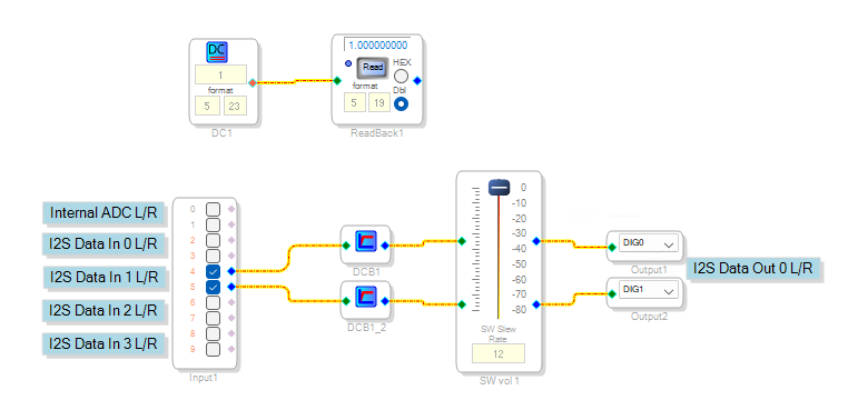
I've not tested this, but with I2S inputs and outputs all supporting slave mode, the DSP can master them all. Here is an example with an additional ADC input and two additional DAC outputs, giving a two stereo in, four stereo out system. Essentially, you are daisy-chaining the devices except for the data wire.
A second ADAU1701 / ADAU1401 board?
Given these DSP boards are less than £15, it is tempting to just use more than one in your project. This expands the IO, gives you another selectable stereo input or doubles the available core instructions, allowing more filters at higher bit rates.
Chaining them is a challenge, and I've not tested this myself.
The easiest way is to connect the analogue output to the analogue input of the second board. This reduces signal quality though as you're making an unnecessary processing through a DAC and then ADC again. Done in this way; most of your processing can also only be in the second DSP too.
It is better to connect the boards through digital IO, but that is also a challenge once again due to the clock speeds of each board being out of sync when they use separate crystals. The Wondom 4-in-8-out YouTube video shows the solution in enough detail, and you can achieve a similar result with these DSP boards, though I recommend buying the Wondom boards for more of a guarantee and making it easier.
To make it work, you must remove the crystal of the second board and send the MCLK to it. Alternatively, send the BCLK output of the first DSP to the MCKI (as well as BCLK input) and modify the second DSP to remove the crystal and modify the PLL pins to both be connected to ground (00).
Expansion conclusion
Expanding outputs is easy and cheap.
If you want to expand inputs, the easiest way in my opinion is old fashioned analogue switches, like a 4-way or more, 2-pole or more pole Lorin rotary switch, relays or a digital switch (like MAX4066) controlled by a microcontroller.
If you want to expand inputs, you can look for modules that support running in slave mode, such as the ones I've confirmed working. This involves no board modifications.
If you're happy to modify, an ADC driving the master clock should work fine, but I've not tested this because I don't like this approach because it will be challenging to daisy chain the fast MCLK to many devices as well as making it difficult to repurpose the DSP later if when it's had its crystal removed.
Be aware of Bluetooth modules though because these may only send the master clock once your sending phone/computer is connected and playing audio. That will constantly start/stop the DSP if used in this way.
Consider the total cost, too. If you're buying the ADAU1701 / ADAU1401 board and then buying separate ADC, DAC modules etc., the cost of an ADAU1452 board with a CS42448 is not a huge jump to get so much more capability.
Overall conclusion
I've opened my eyes to DSP thanks to this board. This ADAU1701 / ADAU1401 DSP board is small, cheap, low power and can really make smaller projects much more versatile. Analogue circuits will continue to be interesting to me, but to make a stereo line level 8-band State-Variable PEQ with adjustable frequency, gain and Q with opamps for example would be massive, needing 32 dual op-amps needed in total, 48 potentiometers, many resistors and capacitors. This would make an analogue solution expensive and noisy if not done right. This little DSP can do all that and brings studio-like control to your own projects.
SigmaStudio is a good piece of software for programming the DSP too. There's no code involved, and you'd even be able to build DSP programs with very little IT or EE knowledge.
I recommend the "How to Sigma DSP" video channel on YouTube and there's also plenty of knowledge on Analog Devices Engineer forum. Both helped me get started quite a lot.
References
- YouTube: @HowtoSigmaDSP by David Thibodeau
- Sure Electronics Application Note: ADAU1701/ADAU1401 DSP Board
- Analog Devices EngineerZone: ADAU1701 Input and Output Signal Routing
- Analog Devices EngineerZone Q&A: ADAU1701 with I2S Slave In, I2S Master Out
- Analog Devices EngineerZone: Setting the PLL Mode for the ADAU1701 at Different Sample Rates
- Pavouk: Modular DAC TDA1543 Information
- YouTube: How to Achieve 4-IN 8-OUT with ADAU1701 APM2