
Building your own PCBs
Contents
Introduction, process and tools
Electronics may begin working point-to-point, on a breadboard, but sooner or later you will want to make your own creations permanent.
A good first step, and one way I still use occasionally, is to build on Stripboard / Veroboard or other type of prototyping boards.
There's no reason a well soldered circuit on these boards won't last pretty much forever, but there are disadvantages:
- Overall board size will be larger due to the restrictive nature of pre-built tracks
- Some components (like Multiwatt style amplifier chips) will not easily fit into these boards without excessive bending of pins, which can lead to damage of the component
- DIP (dual in line) or similar style components will need the strips to be cut properly. Note that DIP style boards do exist, but these will restrict the layout of other components.
- Lots of jumpers might be needed, making construction harder
One alternative is to use software to design a PCB layout for you. Sites such as circuitmaker.com and easyeda.com exist now (but didn't when I started building my own in 2002). These PCB layouts could then be sent to a manufacturer, for a fee.
Many go down this route, but there are some disadvantages:
- The software will have a learning curve
- Your components might not exist in the software. Certainly, many transistor, capacitor and resistor combinations will be fine but that obsolete amplifier chip might not be! There are of course ways of telling the software what the component is, but it takes more time.
- They'll be the manufacturing cost, and time to process and deliver the order
- The above points repeat if you later realise you made a mistake, or want to add a later improvement
- If you're a software consultant/engineer by day like me, you already spend far too much time on the computer anyway!
Designing and building a custom made PCB might seem out of reach, but as I shall describe here designing and building it is not so difficult and it is also quite cheap too. With practice, a simple PCB can be designed, drilled, drawn and etched in a few hours.
There is that satisfaction that you've designed and built the board yourself, especially when it works and actually looks pretty good too!
I think this freehand way of building PCBs is accessible to the novice electronics and DIY hobbyist. It's cheap too, though you do need some tools to start with:
- A plain copper clad board. Budget quality is fine and whilst there are fiberglass varieties that are stronger, they wear down your drill bits quicker. 100 x 220 cm is a good size, but there's no strong preference. Single layer boards are easiest to work with, and FR2 material is fine for this
- Drill bits and Drill for drilling the holes in the board. 0.7mm is a good size for most components. 1mm for others such as TO220 voltage regulators, Multiwatt amplifier chips etc, and 1.3mm to 1.5mm for larger components, such as potentiometers, fuse holders, switches, connectors etc. Get packs of 10 drill bits because these small drill bits snap easier and also go blunt quite quickly. Beware of cheap drill bits, they are not sharp at all and barely work!
- Drill - a Li-ion powered handheld drill that has a chuck that goes small enough will make drilling quick. Hand cranked drills also work, but slower. The ideal is a drill on a stand, but I (still) don't own one.
- A junior hacksaw or whatever cutter you prefer for cutting the board to size
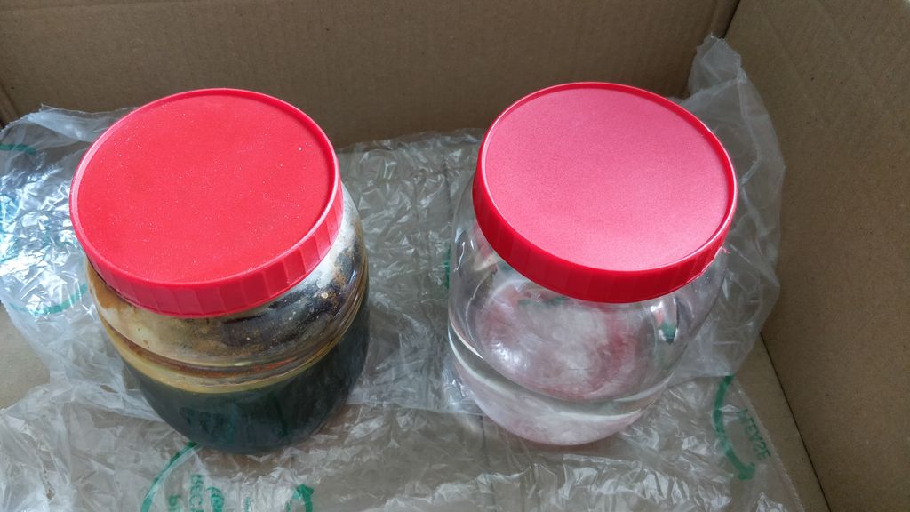
- Copper Etching Solution, such as Ferric Chloride (FeCl3). You can also use a Salt/Vinegar/Hydrogen peroxide mix. The etching solution eats at the exposed copper, but the by-product is toxic, read below for how to dispose.
- A plastic or glass container to store the etching solution safely in. Metal cannot be used!
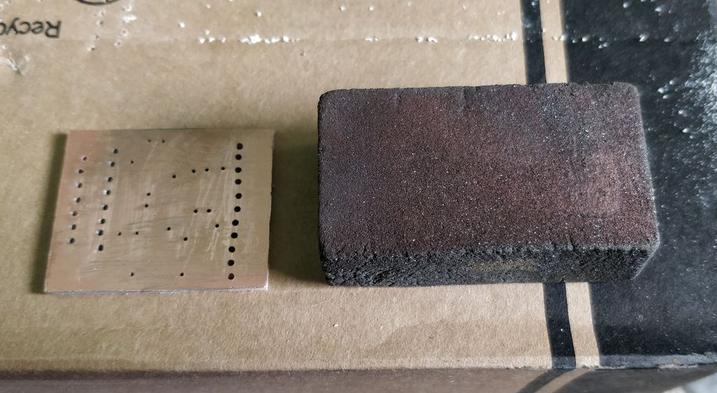
- Copper board cleaner such as an abrasive rubbing block
- An etch resistant pen to draw your layout
- A thinner to clean off the pen after etching. WD40 works!
- Tape is handy for immersing the board and retrieving it after, as well as affixing your layout to the board for drilling
- Rubber gloves for handling
- Solder for soldering after. I use solder containing flux, but if you prefer separate flux then get that too.
- Soldering iron, stand and sponge
- Precision side cutter for removing excess component lead length
- Multimeter for checking continuity of traces, and checking for shorts
- Face protection for protection your eyes, nose and mouth when etching or soldering
That might seem a lot, but most of these tools are inexpensive. The drill you probably already have (but if not, they are a quintessential piece of hardware in your toolbox), as well as the soldering iron and multimeter if you've been starting on electronics previously, meaning the cost of the rest would be £50 to £75 in 2020.
The process of building the PCB will typically be:
- Gather your final schematic. If it's your own design, check again for errors and maybe simulate it (e.g. with partsim.com)
- Design an initial layout using the schematic and the component sizes as guides. I like to do this on paper, which can also act as a drilling template
- Drill the PCB
- Clean the copper side of the PCB
- Draw your layout with an etch resistant pen
- Etch the board with a copper etching solution
- Clean the board
- Draw a topside layout on the board (optional)
- Solder the components
- Test for defects and correct (i.e. dry connections or shorts, traces with no continuity)
- Connect up and test the circuit
Designing your PCB
I design my own PCBs by obtaining the components I need first and then drawing a layout on paper with pen and pencil. You could instead use the software based approach to design a PCB (see links above) and then draw that layout later by hand on the PCB itself if you prefer.
When designing, you need to think about your constraints. Do you want your PCB to determine what enclosure size you need after, or do you want to design your PCB to fit in a given enclosure size?
I've designed PCBs first, but then had to spend many hours looking for a suitably sized project box. Even with the internet and search engines, searching for a project box is really time consuming because you need to look at all three dimensions (internal and external too), wall thickness, material, colour and shape.
Therefore, it is often better to have a think about how much room you'll need for components, then get a case, and design the PCBs to fit perfectly. Think carefully about how many PCBs you need to add, what height they'll be as well as width and depth (some components such as electrolytic capacitors can be quite high), mounting area for controls and connectors, and area for things like heatsinks, transformer, relays etc if needed. A case that turns out bigger than needed isn't a big problem, but a case that is too small can't be made bigger!
You'll have other constraints too, such as:
- Components - think about how much room components will need on your board. Some components need room outside their mounting holes, such as electrolytic capacitors, potentiometers, switches, connectors and things like TO220 and other style chips may need room for heatsinks or other attachments. This is why I will purchase all components first before designing the PCB.
- Edge mounting - your board might have some controls or indicators on it, such as switches/push buttons, potentiometers and LEDs. You will want these evenly spaced i.e. 3 to 5cm between each one. Maybe your PCB is a back mounted board and has connectors on it such as DC power plug inputs, 3.5mm inputs or phono connectors and the like. If your heatsink is mounted to the case, semiconductors that mount to the heatsink will need to be at the edge of the board too.
- Headers - for easily maintenance, you might want to use PCB headers. These will have a fixed width. Ideally, they should be at the edge of the board too for easy access and cable management
- Layout - think about the power flowing through the traces. For a power amplifier, the power rails and speaker outputs need to be thicker. For all types of circuits, the ground should be a thick as possible (or a plane/pour) and not have loops (i.e. more than one path the current can flow down).
- Mounting holes - perhaps your board needs to align to existing mounting holes. Even if not, allow space for them and not just the diameter of the screw you use, but also the diameter of the nut on top.
Once you know your constraints, you can draw a layout on paper.
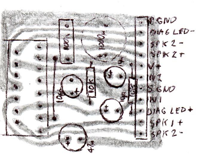
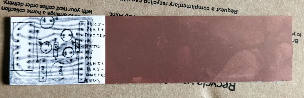
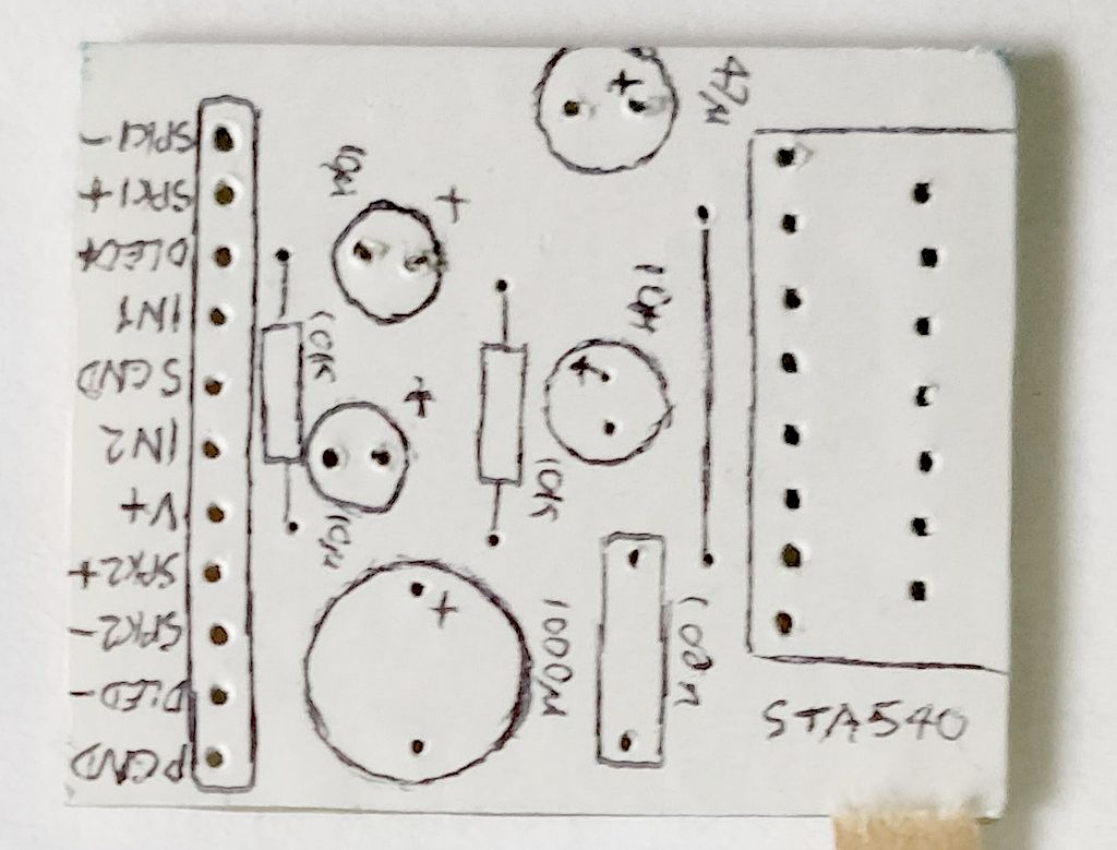
Above: Paper design example for an STA540 amplifier
Start with the constraints - such as your edge mounted components like switches, potentiometers, LEDs, connectors and semiconductors that need to be mounted to a heatsink.
When I design boards, I design it as viewed from the top. This does have the disadvantage of having to reverse (flip) the layout when it comes to drawing it on the board, but it makes laying out the circuit easier for semiconductors because the datasheets almost always show component connections as viewed from above. An 8-pin DIP for example has pin 1 in the top left corner.
The only exception is rear mounted surface mount ICs, which may mean it's easier to design the board as viewed from below. Unless unavoidable though, I recommend against designing a solution for surface mount components because although the result will be smaller and there's no need to drill holes, drawing the layout is really hard, and so is soldering after!
I will show an example of an STA540 / TDA7375 board which only has the chip itself as an edge mounted constraint, so take that chip and push and wiggle it gently into the paper so it leaves marks where each pin is. Then use a pen to make each indent clearly visible for layout and later drilling.
If you don't have the IC yet, the datasheet will have dimensions so carefully measure them out with a ruler and mark where the holes need to be.
Now I can start drawing the traces with pencil. The reason I use pencil is because it's easy to grab a rubber (eraser) and change my mind on a layout or correct mistakes. This also contrasts between the white paper, and the black pen used to mark the holes and component overlay.
Think about what traces to draw first. Chances are if you have a semiconductor in your circuit, it will need bypass capacitors. Bypass capacitors are those between the ground and the power supply rail(s) and will be a ceramic (or MLCC) capacitor of around 100nF to 1uF, and a larger electrolytic capacitor of 47uF to 470uF or more.
The smaller ceramic capacitors need to be as close to the semiconductors IC as possible, so that will probably should be the next component to mark on your board and draw traces to.
The larger electrolytic capacitor can be further away, but again closer is better, so perhaps do that next.
As you layout these components, they'll probably be going to 0V ground, so you can think about your ground layout and how this should eventually form a star point, or perhaps a ground pour or plane if you use a dual sided board is better.
Now start laying out the rest of the circuit. Most capacitors often have a fixed spacing for the mounting holes (especially polyester and electrolytic), as do transistors, headers, connectors, switches, potentiometers and of course other ICs, so measure these and mark out where the holes will be first.
Typical spacing is 5mm, 7.5mm and 10mm for most capacitors. Remember electrolytic capacitors are a cylinder so don't mark out locations for other components too close to them.
Resistors and other types of capacitors (axial lead, or ceramic) are more flexible. The ideal resistor spacing for common ¼W is 7 to 10mm, but they come with long leads so you can go longer if you need them to bridge a large gap. If you need them to bridge a smaller gap, you can mount them vertically instead in a gap of 3mm or so.
I find it helps after marking the mount holes to draw an outline of the component on the paper design, as well as the component value or code (R1, R2 etc). This helps retrace the design as I go and also helps placing the next components to know where there is space on the board so components do not cross each other or pass space occupied by a large component such as a capacitor, potentiometer and so on.
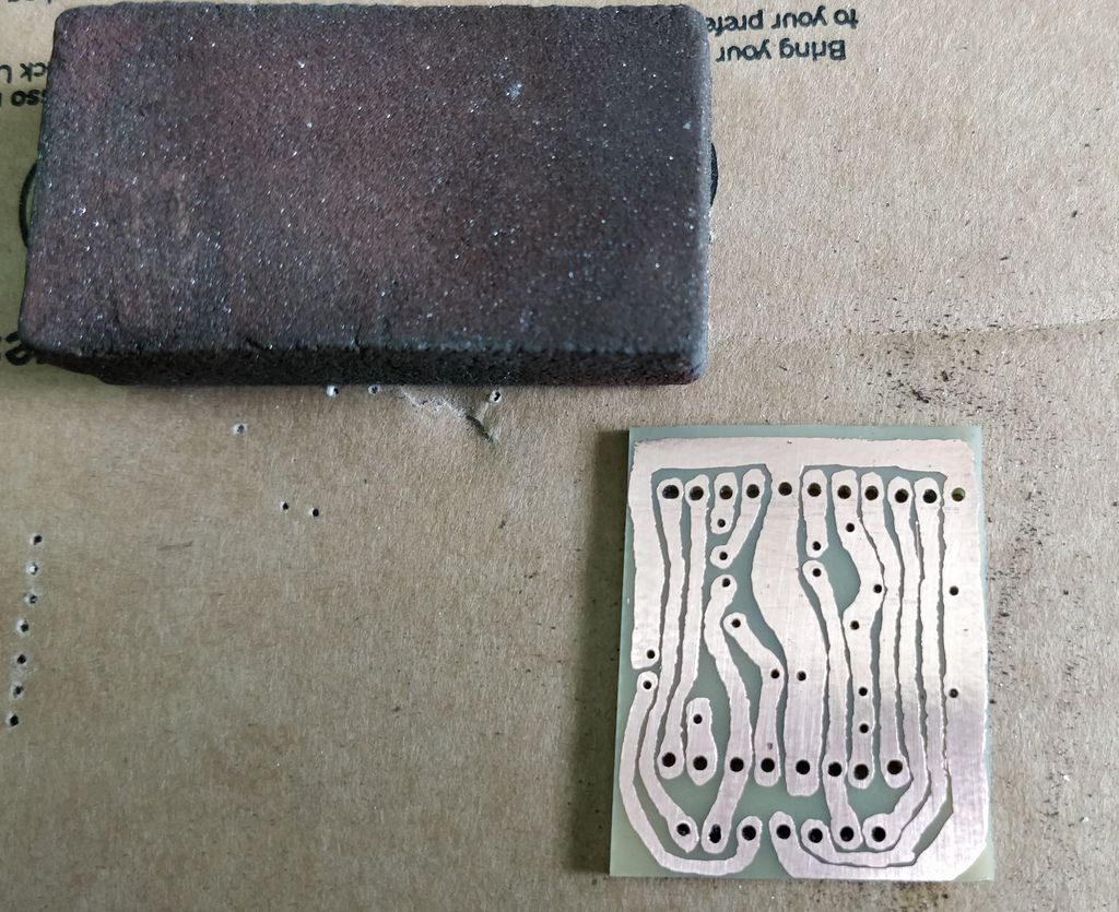
On single sided PCBs, it might not be possible to layout all traces without them needing to cross each other. If you do get away with it, you've done really well, but almost certainly a jumper or several will be needed to make the connection. On my STA540 example, connecting pin 3 to pin 13 would either need a long division to go around pins 4 to 12, which would then need another bypass capacitor for stability since it's a power rail. The alternative is to make a jumper over the other traces to simplifier the layout. When soldering, the jumper can either be a wire, or the offcut from a resistor lead if it reaches.
Once you've drawn all traces - double and triple check the layout. I usually make a mistake on more complex circuits, either missing a trace, or a trace going to the wrong component and correcting them in the paper design is easier than correcting it later on the PCB itself.
Once you're happy, scan your design or take a photo of it. Using image software, do a flip horizontal (or vertical) and you've now got a copy that's perfect for drawing the layout on the copper board itself. You can then work from the computer or mobile screen to draw the layout or print it.
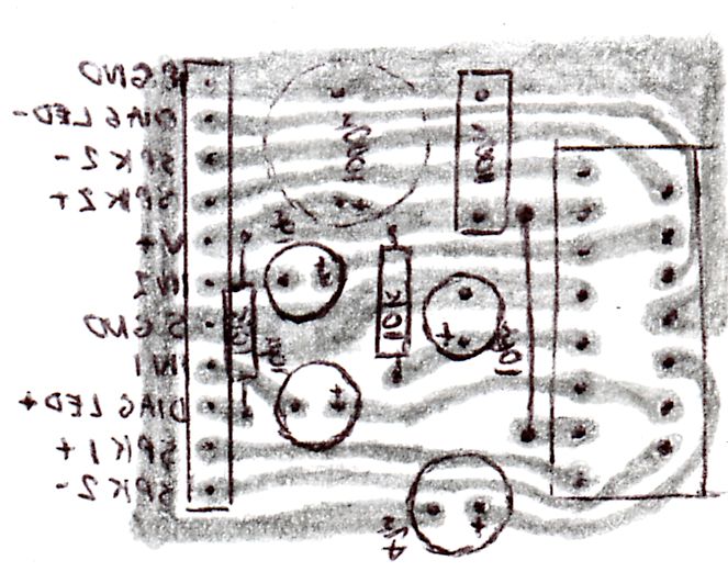
Above: Paper design flipped/mirror horizontal
Drilling the board
Use your paper design as a template / guide for drilling. I drill first before drawing the layout because:
- The holes give guidance to draw the layout (a bit like dot-to-dot drawings you did as a child!)
- Drilling after marking the board will scratch the pen markings, ruining the etch
If you have a scanner and printer, you can scan your layout, flip it and then print in DPI/exact size to produce a flipped 1:1 copy which is perfect for drilling the copper side of the board.
If you don't have a scanner but do have a printer, doing the flip of the photo and then cropping carefully and printing with software that lets you specify the photo width can also work, but there is a risk of slight differences (measure after printing).
Another way (also if you don't have a printer) is to grab a sharp point (such as the point of a compass) to punch small holes in your paper layout where holes need to be drilled and then once this layout is reversed, it can be taped to the copper side of the board as a guide.
Above: Affixed mirrored template
Drilling the board takes a little time because you might end up with 100+ holes to drill. When drilling, especially with sub 1.5mm drill bits, apply only a little pressure downwards, and no pressure sideways! That's because these drill bits are brittle and snap easily. Be patient and you may still snap some drill bits so have spares. With practice and an electric drill, you'll still be able to drill a 0.7mm hole in just a couple of seconds.
I suggest drilling the copper side of the board. If you drill the non-copper side, you'll get some tear out in the copper when drill bit punches through. Adding some material underneath and clamping to create zero clearance might help, but will blunt your drill bits faster.
If your drill bit is sharp, the tear out might not be too bad and you could use a small chisel to remove the excess, and clean up with a cleaning block, but you still risk some tear making the hole on the copper size bigger than it should be, which complicates soldering later.
Before drilling the holes, think about the diameter they need to be. Most resistors and capacitors suit 0.7mm holes, but larger more powerful ones might need larger holes. If you don't have or cannot obtain 0.7mm, up to 1mm still works, but soldering will be harder after.
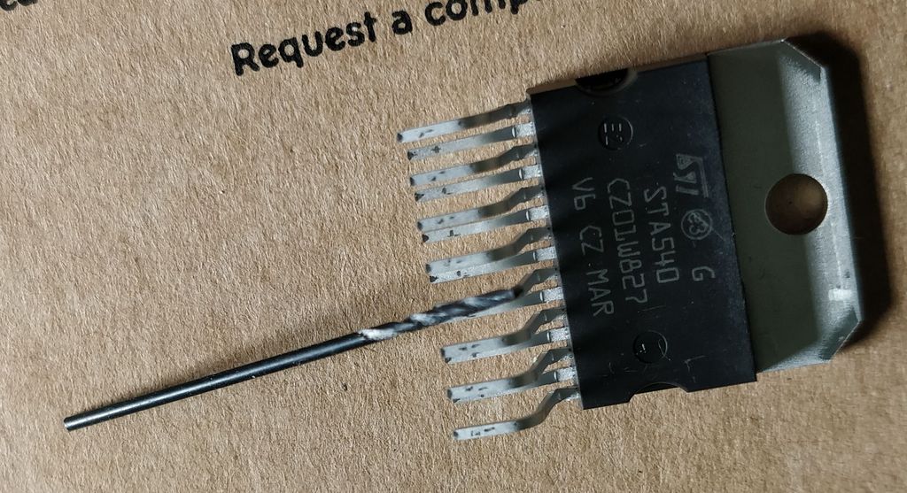
Above: Comparison of 1mm drill bit to STA540 pins
TO220 transistors, voltage regulators and other style ICs usually suit a 1mm hole fine. PCB headers also suit 1mm fine. Connectors, potentiometers and other larger components may need anything from 1.2mm to 2mm.
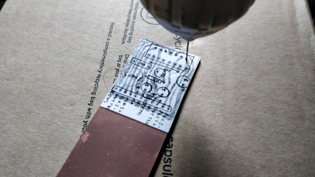
Above: Drilling into the board via the template
Once you finish, check the layout again to ensure you really are finished. I sometimes miss a hole or two myself on larger boards. It's easier to drill them now when you can use the template rather than later.
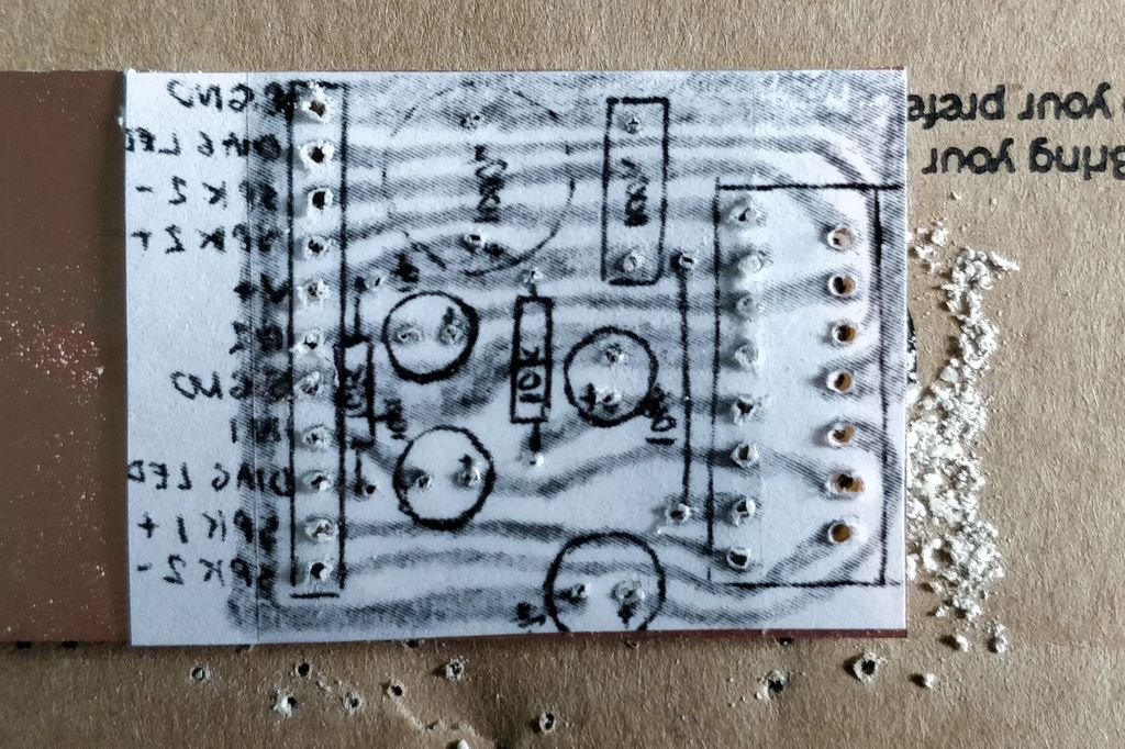
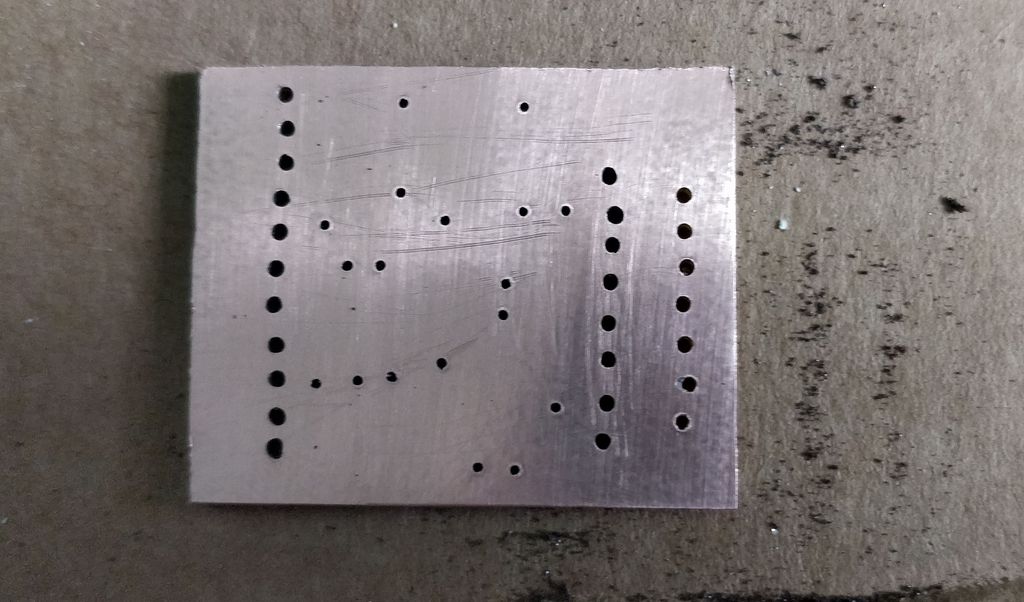
Above: All holes drilled with template still attached
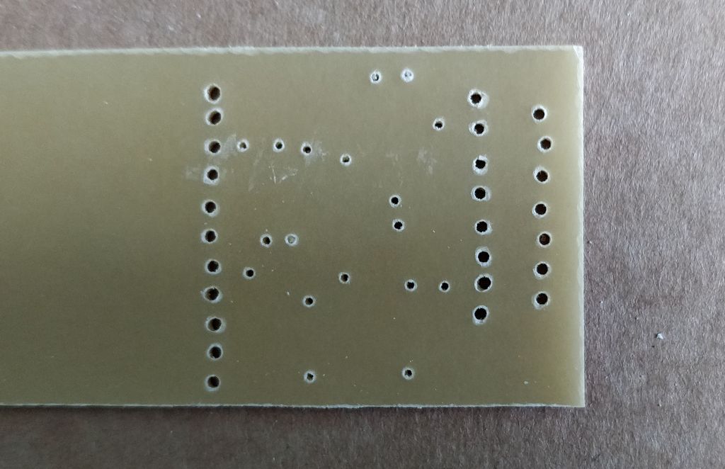
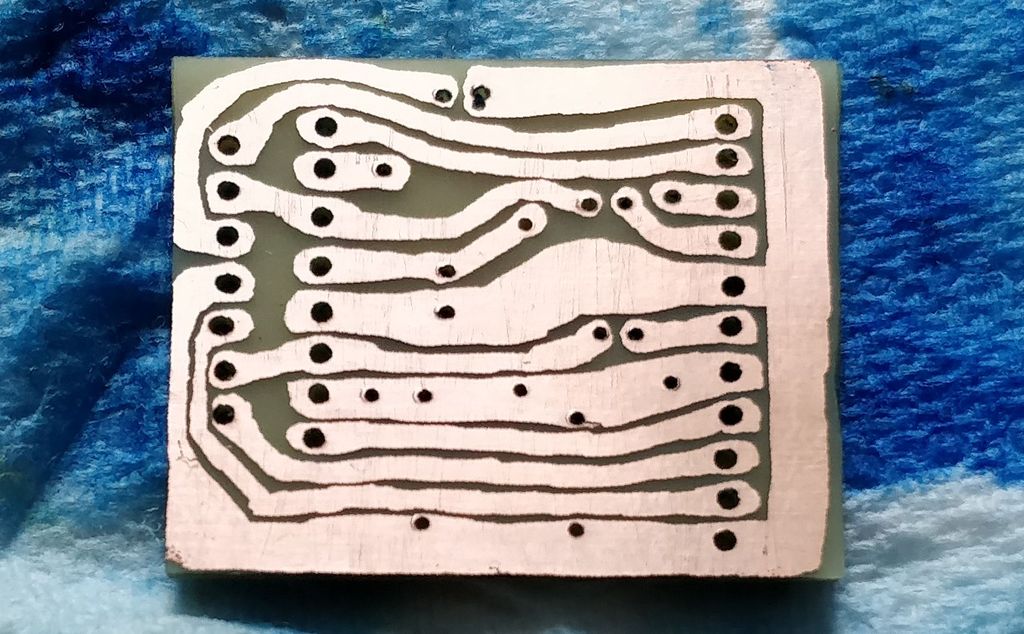
Above: All holes drilled with template removed. This is the front side of the board, where the drill bit exits.
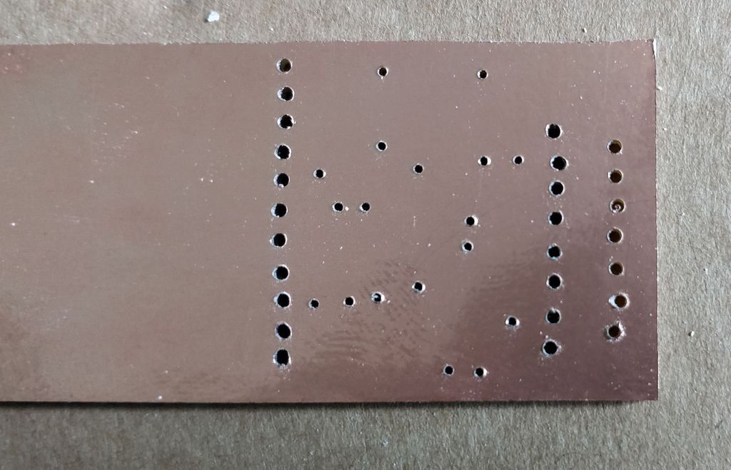
Above: All holes drilled with template removed. This is the copper side of the board.
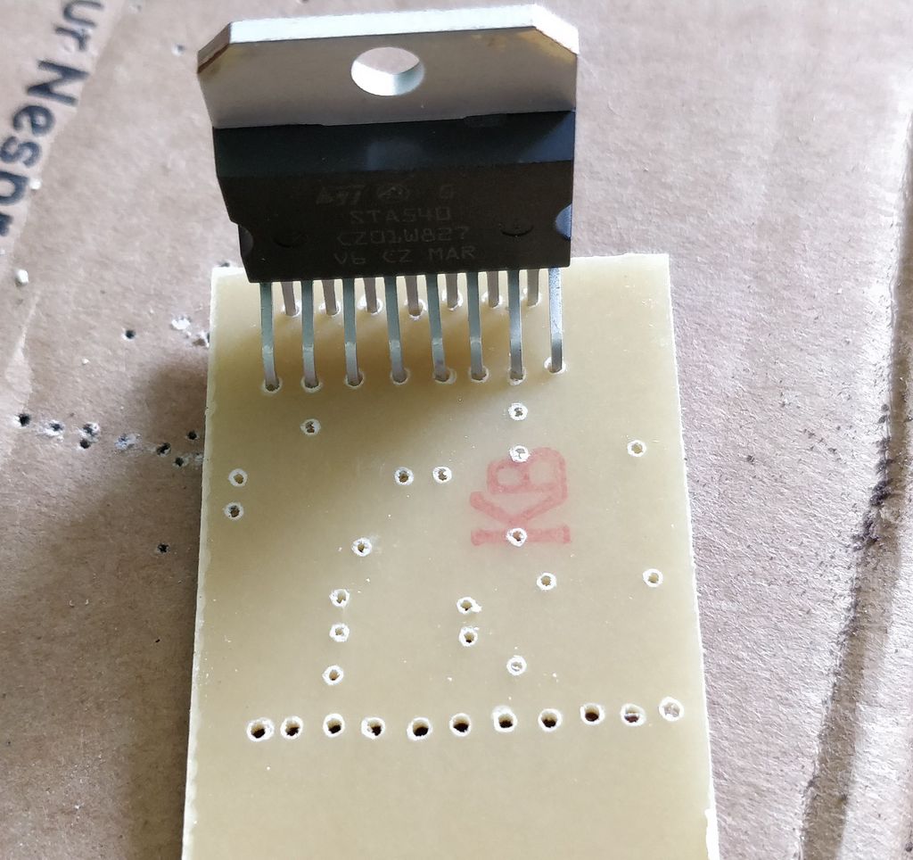
Above: It's a good idea at this stage to check your components align with the holes too'.
Now that drilling is complete, if the board needs to be cut, it can be cut to size now. I prefer to cut with a junior hacksaw, with a metal blade in it. Cutting at a shallow angle like shown below helps ensure the cut is straight.
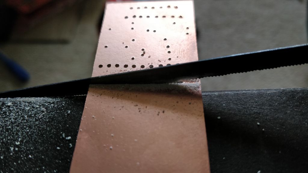
Above: Cut the board to size. I prefer a junior hacksaw.
Drawing the board - applying the etch resistant pen
Before starting, ensure all holes are drilled and the PCB has been cut to size. If you do this after drawing the etch resistant layout, you will risk scratching it off and will need to reapply.
Before drawing, also clean the copper of the board using an abrasive cleaning block. This ensures the pen ink sticks nicely to the copper, and it etches easily after. Don't use a wet cleaner otherwise the residue liquid will cause the ink to run and not stick properly.
Before rubbing the board with the cleaning block, you might still have some sharp tear out at the holes, even if you drilled on the copper side. Remove these first with a chisel or something sharp and flat and then clean with the cleaning block.
Above: Board scrapped, ready to be cleaned
Above: Board after cleaning
After cleaning, the copper on the board should be shining - almost like a mirror. This gives you the best surface for drawing on and etching.
Get your flipped layout ready. This is what you'll use to draw the layout from and double check to ensure that you're really looking at the flipped layout as a guide and not the original (assuming your original was designed as the top view of the board). A printed copy is the most handy to copy from, but you could draw from your (well charged) Smartphone instead (just turn off the screen auto power off), or a computer monitor if you don't mind moving your eyes more during the copying process.
Shake the pen and using the pre-drilled holes as a guide, copy the layout carefully. If ink is not flowing enough, you can usually push down on the tip to get some flowing, but do this on an area of the board where wide traces are needed (such as the ground traces) in case lots of ink flows out. Safer still - do it on scrap paper (folded several times so the ink doesn't soak through).
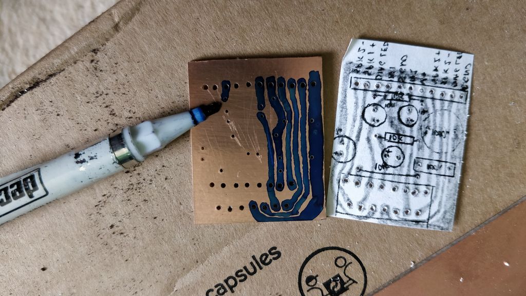
Above: Drawing the layout from the template with the etch resistant pen
As you draw, start in the top left and work down and right as you go if you are right-handed, or top left to right and work down if left-handed. This avoids smudging the ink with your hand. Shake the pen periodically to ensure the ink consistency is optimal.
To also avoid oxidising the copper board, I also suggest placing a piece of paper to cover any area where you need to rest your hand as you draw if it is over a copper area. If you don't do this, the sweat on your hand will oxidise the copper a bit, making the it hard to draw on when you get there and also slower to etch later.
The tips of these pens are usually not precise, so if you've designed any thin tracks you might have to draw them thick and touching other traces for now and then when the ink dries, use something sharp (like a bradawl) to scrape away the excess ink until the copper below is clearly visible again.
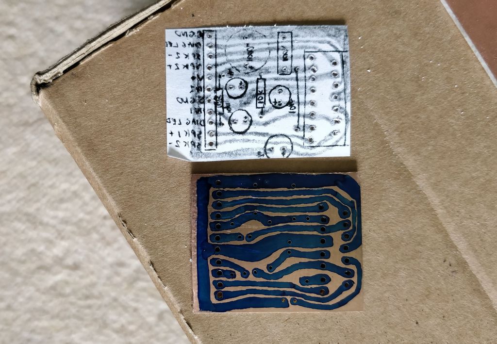
Above: Completed layout drawn
Once you've completed your layout, allow some time for the ink to fully dry (I usually wait 30 minutes). Double check for any ink runs which could have joined traces together that shouldn't be and scrap them away if needed.
I suggest etching the board as soon as possible after the ink is dry otherwise the copper will oxidise over time. I have etched boards a day after drawing them, but the results are never as good.
If you do need to etch it later, store it in an airtight bag to restrict the oxidation and be very careful not to touch the ink because micro-scratches can occur and these create hairline breaks in your board which ruins the layout somewhat (they can be corrected by bridging with solder, but it's inconvenient!).
Etching the board - using the copper etching solution
Happy the layout you've drawn? It's now time to etch it!
Safety / First Aid
| FERRIC CHLORIDE IS VERY CORROSIVE, ESPECIALLY TO METALS. Do not get this solution on hands, clothes, surfaces. Do not pour it down drains or sinks after use without making it safe first. Seek medical advice immediately if any solution gets in eyes or mouth etc. |
- If the solution gets on your skin, wash with lots of water. If it is still affecting you, seek medical advice.
- If the solution gets on your clothes, remove them and wash with washing soda which will neutralise the chemical even if you intend to dispose of the clothes now that they're stained.
- If the solution gets in your eyes, irrigate with cold running water immediately, then seek medical advice.
- If the solution is swallowed, seek immediate medical aid. That's a 999 / 911 call.
- Spills should be washed with washing soda and mopped up with paper towel such as kitchen towel.
Despite the danger, safe use of this chemical should not cause you any problems. These guidelines give you a quick description of how to make it but I strongly suggest you read up more on this topic so it is specific to your etching solution that you brought if it is not Ferric Chloride.
Along with pre-cautions above, I also recommend these actions are also taken when using this chemical:
- Wear old clothes. If you get a slight drop on your clothes, there is no way that you will be removing the stain, whatever cleaning agent you use. A small yellow stain will always be there. Even if disposing after, wash the clothes with washing soda (not standard washing powder/detergent)
- Never get this chemical near metal. That means do not wash it down sinks, drains or anything like that - it will corrode them and ruin them, particularly aluminium
- Discard the spent solution safely (see below)
- Avoid the kitchen - the by-product is toxic and should be kept away from food or anything that is used for food preparation
Most versions of ferric chloride come in bottles or as rock crystals. I have not used bottles yet, but a bottle will contain about 250ml of the solution and will probably need to be diluted, to make 500ml usually. Follow the instructions on the side of the bottle for specific details (I am not providing these). I prefer to buy the ferric chloride crystals (or "rocks"). These come in a bag with the instructions on a sticker (read them :P) for how to dilute and use.
The crystals I but come in a 250g pack. Again read the instructions for your specific product, but usually the method is to add these crystals to half a litre of warm water and stir rapidly with a wooden stick or plastic spoon that can be discarded after (or better stored safely kept for reuse next time). Never use anything metal for stirring, or anything you intend to keep clean and use on something else. At first sight, it doesn't look like the crystals will dissolve at all (as they are huge), but warm water and continued stirring, they soon disappear. The result is a very orange looking amount of water - this is your etching solution. ferric chloride is also available as anhydrous ferric chloride. I do NOT RECOMMEND this, and it should be avoided for these reasons:
- It's undiluted without any water content. It is a powder. Powders can be easily breathed in and since this chemical is poisonous, it's hard to recommend.
- When mixing it with water, lots of heat is produced. The energy released by this chemical can heat up cold water to a point where it can melt some plastic containers
- Although the above statement seems to imply the chemical dissolves well, it does not. It easy to have lots of powder that won't dissolve, and you get a solution that looks like it should work, but actually doesn't
Since anhydrous ferric chloride is hard to recommend, I will not give details about using it.
I suggest that if you are etching your own board for the first time that you do a small board to practice with. For my first test, I made a small board for a power LED which is basically an LED, a small resistor and two holes for the power wires. If you do this successfully, then you may move freely to bigger boards, although I still wouldn't suggest anything huge if you are a beginner.
Etching
Above: The ferric chloride solution and rinse water in a lined box
Now you are about to etch the board, if you have not done so before, prepare the etching solution or reuse your existing one.
Give it a quick shake or stir (naturally the container it is in must be tight) and transfer it into a container that you will use to etch the board in, or if your board is small enough, you can etch it in the original container to reduce the chance of pouring accidents.
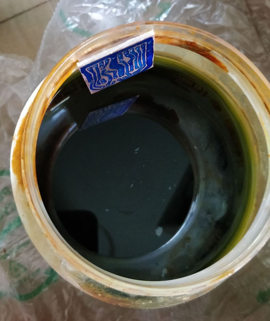
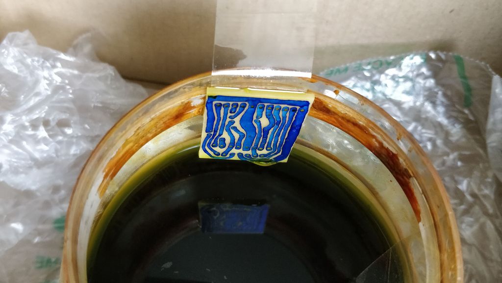
Above: Tape the board, then sink it in
I affix tape to the bare side of the board (without copper) for retrieval of the board after. A piece of thread through one of the drilled holes is another way. Then the board can be bathed in the solution.
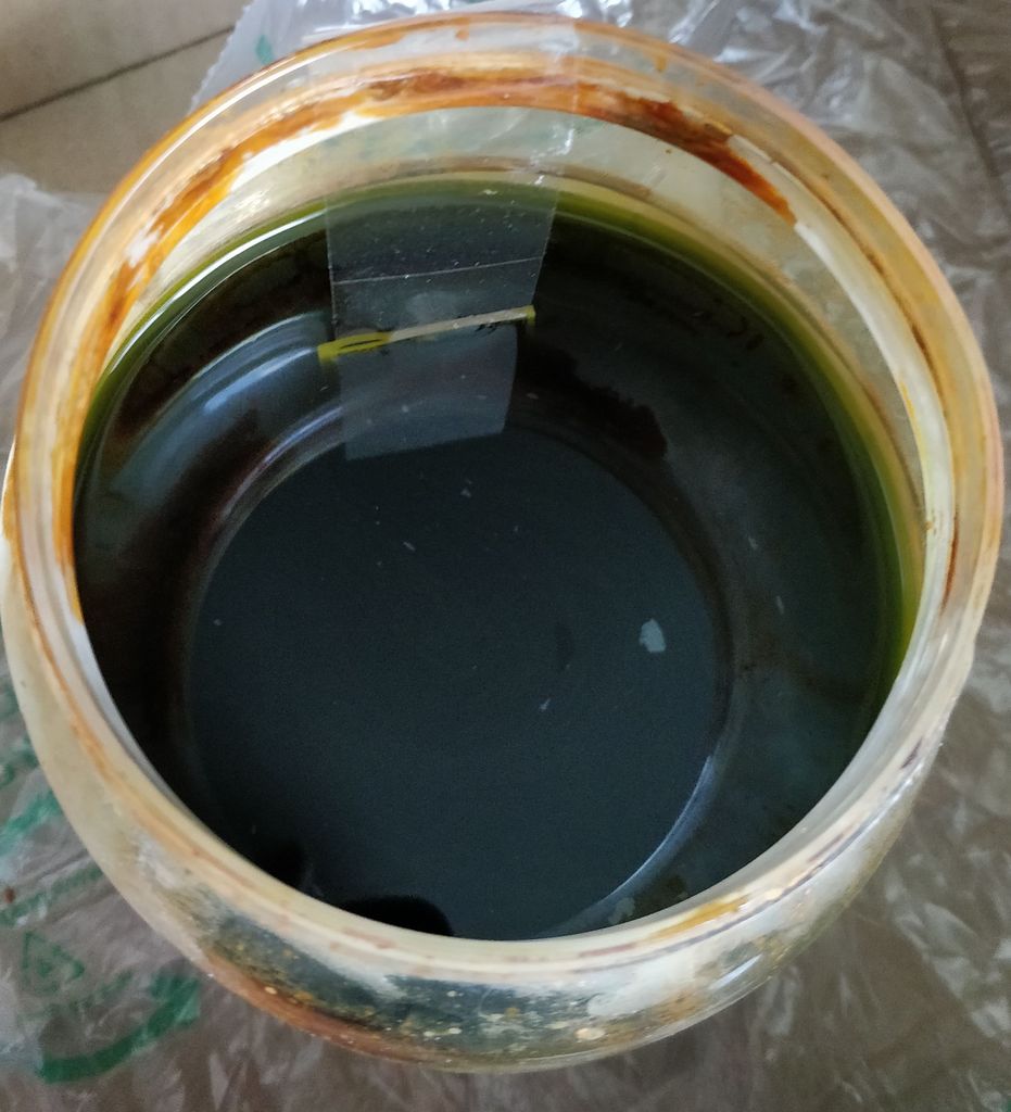
Above: Board sunk into the solution - keep it as close to the top as it etches faster
Secondary school chemistry probably taught us that reaction speed can be increased by temperature/movement, concentration, particle size or use of a catalyst.
We can use the temperature and movement hear to speed up the etching process, so pre-heating the solution a little (do not use the microwave!) will help, and movement of the liquid during the etching process will also helps, such as stirring, rocking or dipping the board in and out.
If you don't want to sit and stir/rock the solution yourself, you can go away and just leave the board to etch longer. It will eventually complete. Or make a little something to rock gently or vibrate the container with a motor.
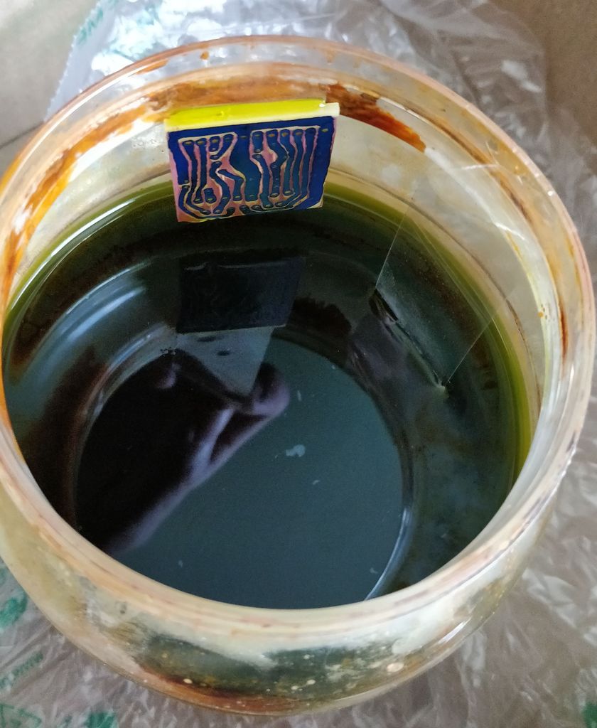
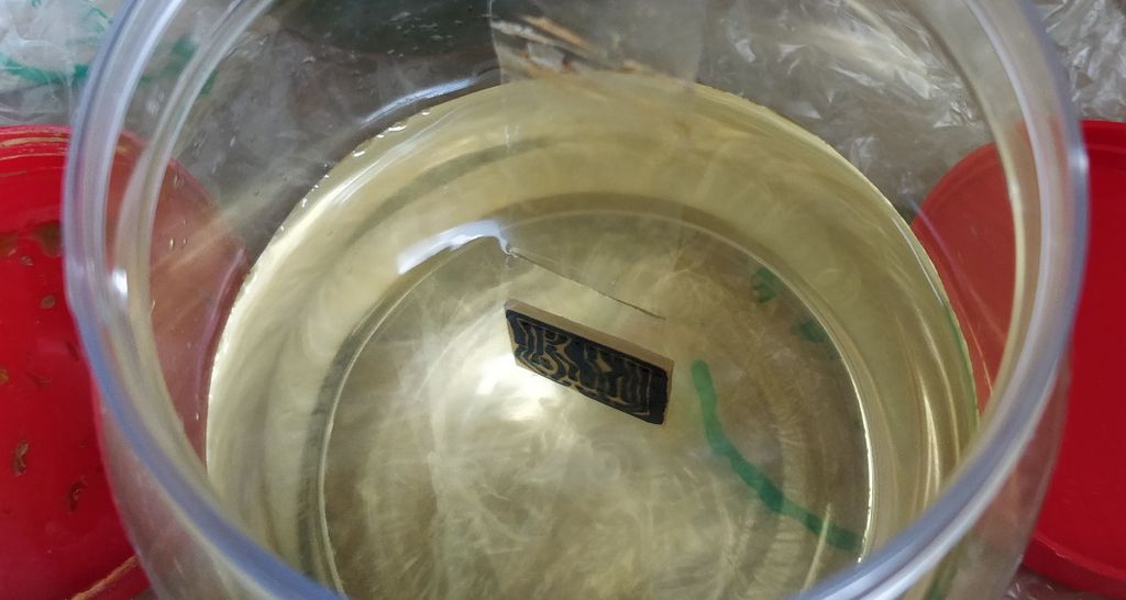
Above: Partially etched - not ready yet, but almost!
On a cold winter day, with a somewhat spent solution though, it could be an hour or more you'll need to wait, which risks the pen ink drifting off, so check regularly.
If bathing horizontally in a tray, I suggest rocking it regularly otherwise air bubbles might prevent copper from being etched. To minimise air bubbles, etch copper side facing up.
On a warm day with fresh solution you might etch in less than 5 minutes even without stirring - so watch out! If you leave the board in there too long, the etching solution will start to eat away at the protected areas from the side where the copper has now been removed, or the pen ink might drift off.
Concentration is best not controlled. The concentration of a fresh solution will be best but etching the board and then creating a fresh solution every time is very wasteful so reuse the solution as long as possible. It will get slower over time though, and eventually stop working, but that's after making many boards.
Monitor regularly. If bathing vertically, the top of the board will etch before the bottom so you may need to raise it upwards during the process. Once fully complete, it's time to remove.
Above: Fully etched - time to remove
You should remove and place the board in another container for cleaning. Fill it with water. Lift the board out of the solution and shake it gently to let as much etching solution drip back into its original container as much as possible. Don't shake violently otherwise droplets can ruin carpets, surfaces, clothes or worse get in you're eyes etc - though you should wear face protection to prevent this.
Place the board in the container with water and rinse it around. Once the board looks quite clean, now you can use a thinner to remove the etch resistant ink. WD40 (other brands are available) works well, but also paint thinner. Spray or dip it on and clean with disposable paper towel (kitchen towel works well).
Above: Rinse in water
Rise once more, and dry. The board is now ready.
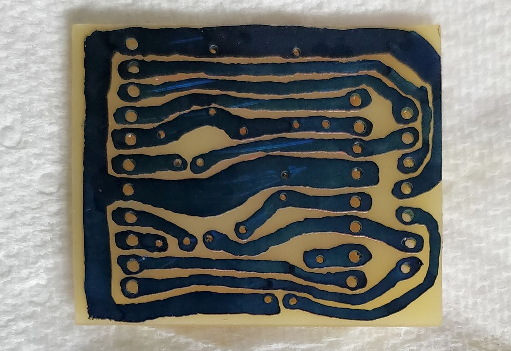
Above: The completely etched board, but still with etch resistant pen ink
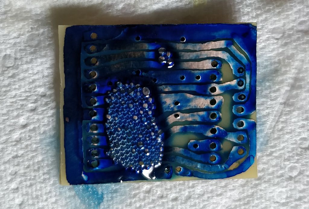
Above: WD40 thins the pen ink quickly
Above: Board cleaned of ink
Etching Solution Disposal
The residual copper in the etching solution and the rinse water is an environmental hazard and should not be disposed of by pouring down the drain without first making it safe.
To make it safe, use sodium carbonate (washing soda) or sodium hydroxide added slowly until it is no longer reacting and the pH is greater than 7. Adding pieces of aluminium foil can also be used to neutralise it.
Once neutralised, the remaining liquid can then be diluted and poured away and any sludge remaining can be collected in bags and disposed of as appropriate for your town/city authority. London (UK) has a free Hazardous Waste Collection and Disposal Service.
Mark-up
This is not strictly necessary, but I usually mark-up my board before soldering by placing a white sticker over the plain side. This has to be a heat proof sticker otherwise the sticker will blacken when soldering.
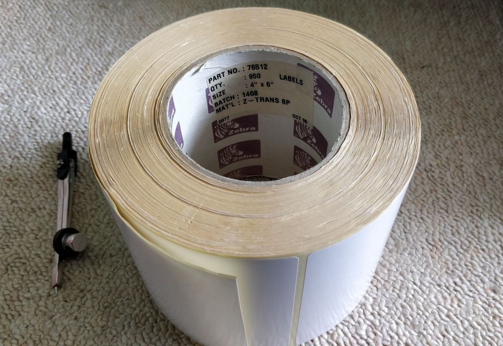
Above: My sticker roll, from 1996!
I'll stick a sticker on the board, use a penknife to cut off any excess at the edges and then use a small point (such as the point on a compass) to punch through the sticker where the component holes are. The holes can be found by holding the board up to a light.
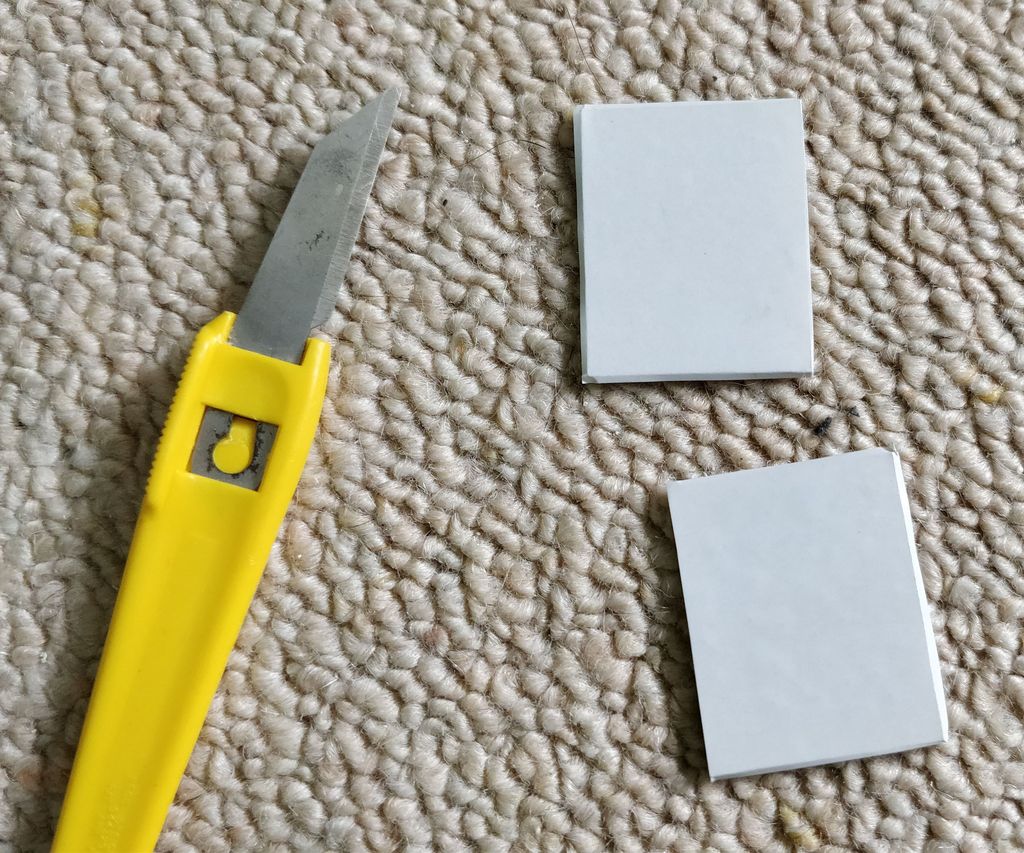
Above: A penknife is ideal for trimming the edges
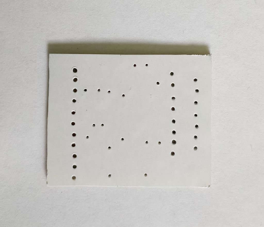
Above: Holes punched through the stickers
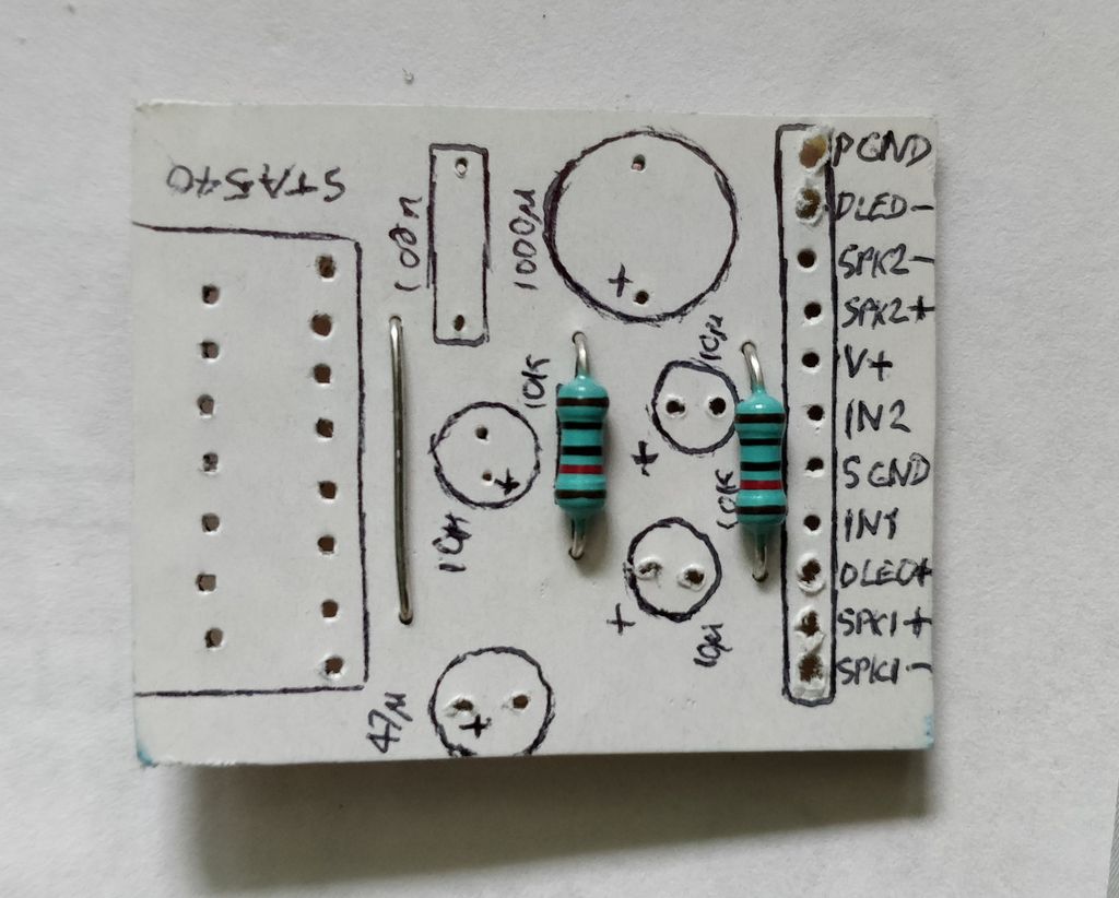
Using pen, I'll then draw on the components and their values. This makes soldering easier because I don't have to look back at the paper templates to see what goes where and reminds me of values if I lose the template.
Above: Mark-up drawn
Soldering
Before soldering, inspect your board. If there are any traces which are bridging to others because the copper was not fully etched, correct this by making a gap with a penknife or similar. Check for continuity with a multimeter where it should be, and check all adjacent tracks where there should not be continuity to confirm that is so.
If there are any traces which should have continuity but do not - this may be an over-etched board or there may be a scratch on the trace. It's not necessarily a disaster and may be recused by bridging any gaps that shouldn't be gaps with solder.
Above: Cleaned board ready for soldering
If you left it a day or a few in between completing the etching and starting the soldering, you may need to rub that abrasive cleaning block over the copper again. This ensures the solder makes good contact.
I find soldering (and de-soldering) my DIY boards much easier than soldering Stripboard / Veroboard. The wider pads and greater space between pads ensure a good joint connection and also reduces the chance of solder flowing on to adjacent traces, bridging the two and probably causing a short circuit. This is a common pain with Stripboard / Veroboard where the traces can be easily accidentally bridged with solder which can be hard to correct.
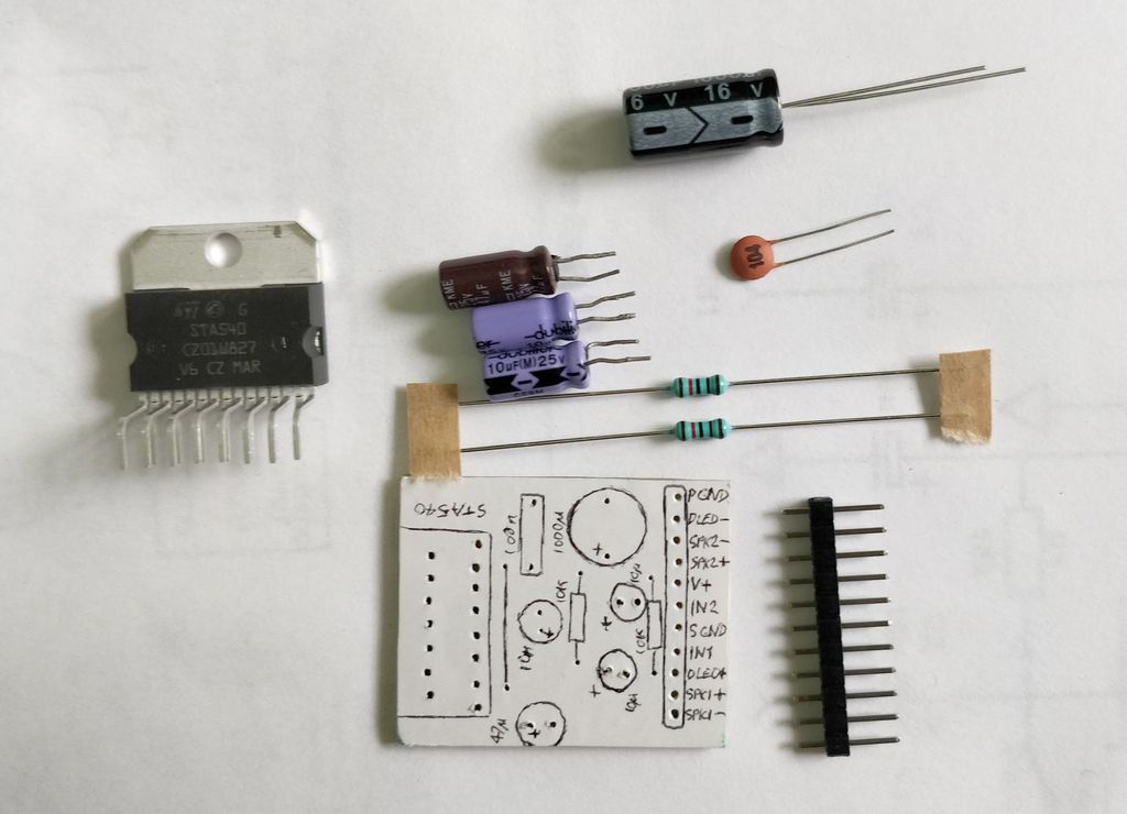
Above: Components to solder
There's plenty of guides online for how to solder, but really my technique is to:
- Find all your components first to avoid having to dig through boxes to find the components you need
- Start by placing 5 to 10 low height components such as resistors and diodes on the board
- Solder each joint by applying heat to the copper trace for a second or two, then the component lead for less than a second, then add the solder. Do one joint for each component, then come back to do the second joint to allow the component to cool first.
- Remove the iron as soon as the solder flows and creates a joint between the two
- If it doesn't after three or four seconds, remove the iron and try again after the components cool
- Cut off excess leads lengths as you go, otherwise they tend to get in the way when soldering other joints
- Do any jumpers after you've done resistors, since you'll now have lead offcuts
- Any low height ICs or their sockets can be added and soldered - don't solder every pin at once, let the IC cool down for a few minutes once it starts to feel warm
- Then PCB headers
- Then capacitors and/or vertically mounted resistors and/or transistors
- Then larger components such as high height / vertically mounted ICs, connectors, switches, potentiometers and the like
After soldering, do a board test with the multimeter. Any good one and even basic ones should have a 'Continuity' tester, which is the symbol looking like sound waves.
Touch the two probes together - a tone should be emitted by the meter. This confirms the function is working and selected properly, probes plugged in correctly and so on.
Then check the traces. Check the beginning and end of each trace - there should be continuity (and a tone). Now check adjacent traces. There should be no continuity. Do note though if you've soldered any low value resistors (like 10 ohms give or take), they may show up as continuity. You can measure resistance instead to confirm there is no short.
If you do have continuity / shorts where there should not be any, check the solder joins are not spilling over to adjacent tracks and use the soldering iron to drag the excess solder away if you can or apply de-soldering braid to remove the solder and redo the joint carefully.
If the continuity is still there, it might be the traces are too close together and a small amount of copper is touching between the two traces. You can use a penknife to cut between the traces, and recheck with the multimeter continuity setting to see if the problem is resolved.
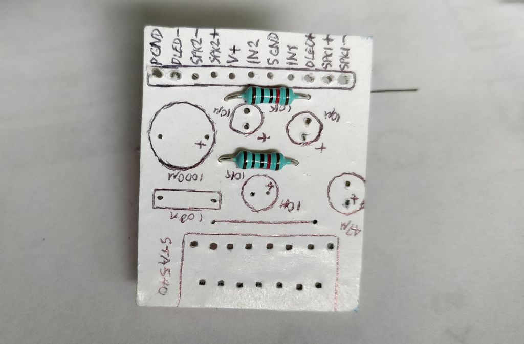
Above: Resistors placed
Above: Resistors placed, underside
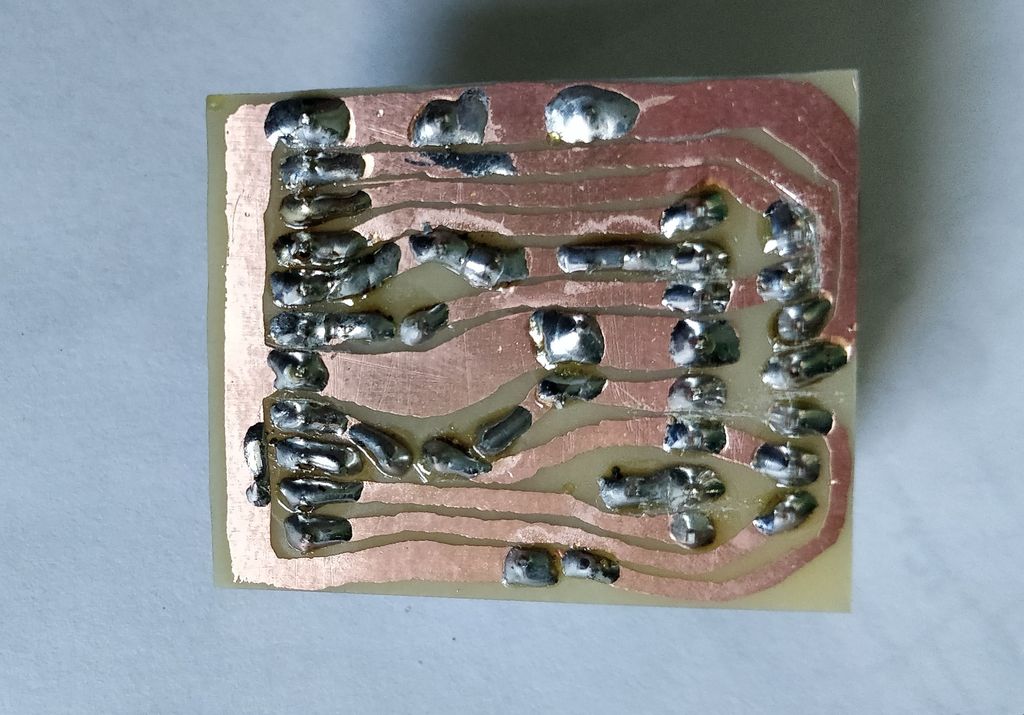
Above: Resistors soldered, underside
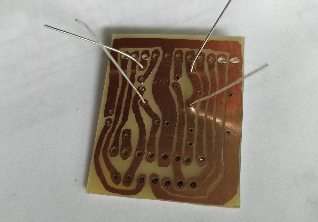
Above: Jumper soldered
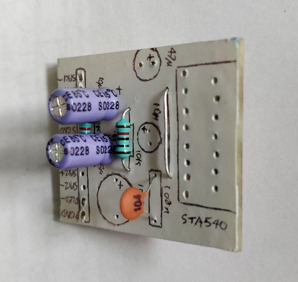
Above: Capacitors soldered
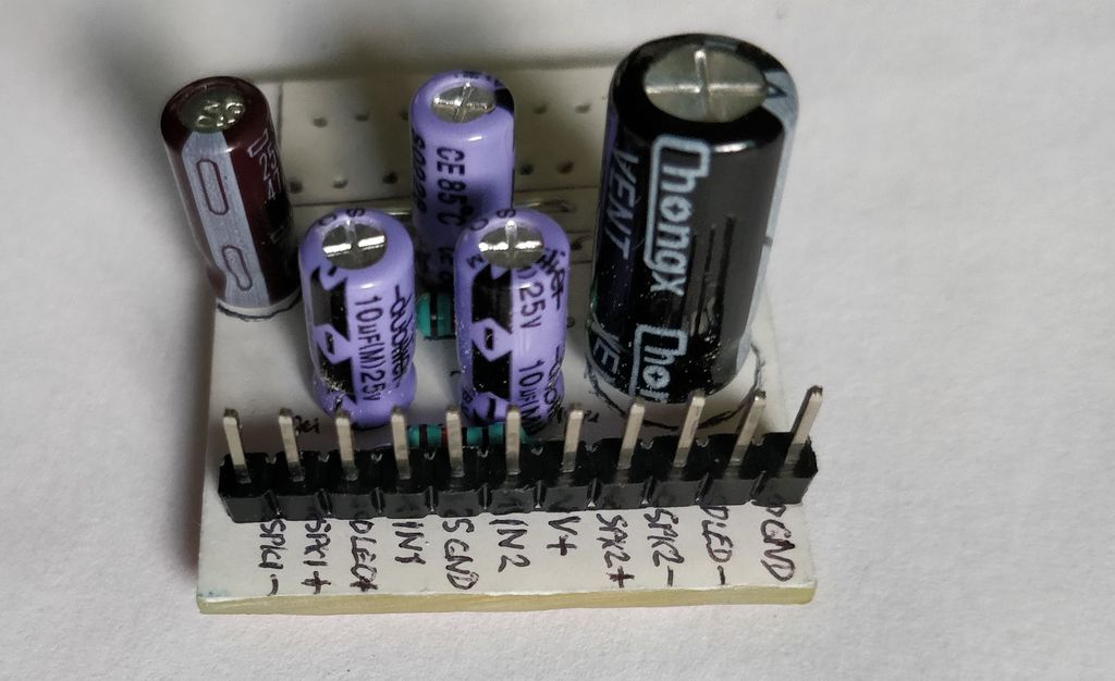
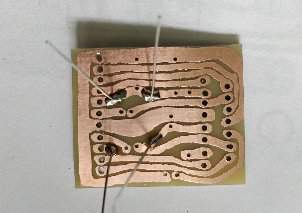
Above: Header and capacitors soldered
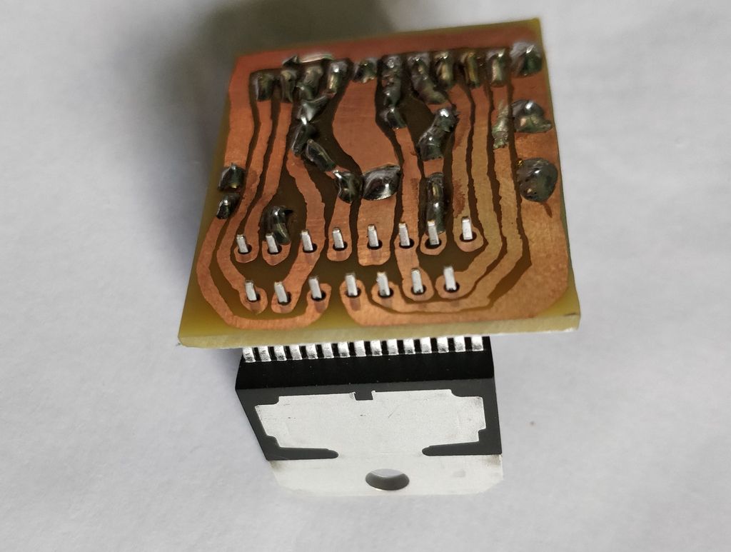
Above: Integrated circuit placed for soldering
Above: Soldering complete, underside
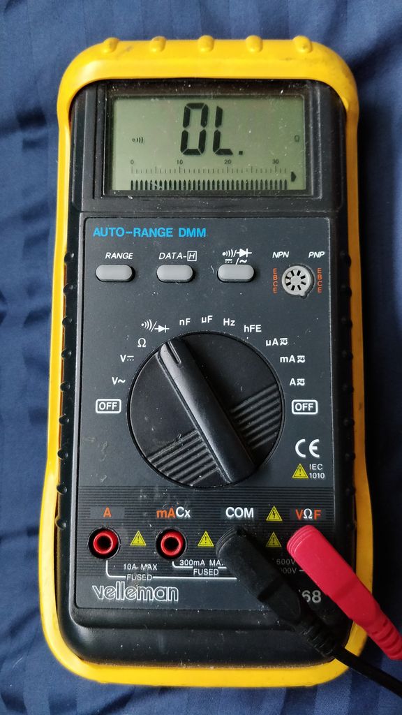
Above: The multimeter 'continuity' setting is useful for checking traces. It beeps when there is a circuit.
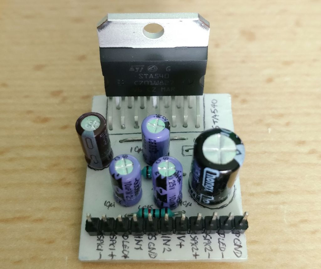
Above: Completed board (minus heatsink)
Finally, you may solder the connection wires to the board and test your circuit, if all is fine, congratulations. Otherwise you will need to go back, check your circuit designs, check your soldering and board construction and check whether all your components are in the right way. Good luck
References
- Ferric Chloride - Prototyping | MG Chemicals https://www.mgchemicals.com/products/prototyping-and-circuit-repair/prototyping/ferric-chloride-415
- How to Design and Make Your Own PCBs by R.A. Penfold (Babani Electronics Books) ISBN 0-85934-096-1
- ESP: www.sound.au.com
- Hackaday - Testing the efficiency of PCB etchants https://hackaday.com/2014/05/08/testing-the-efficiency-of-pcb-etchants/